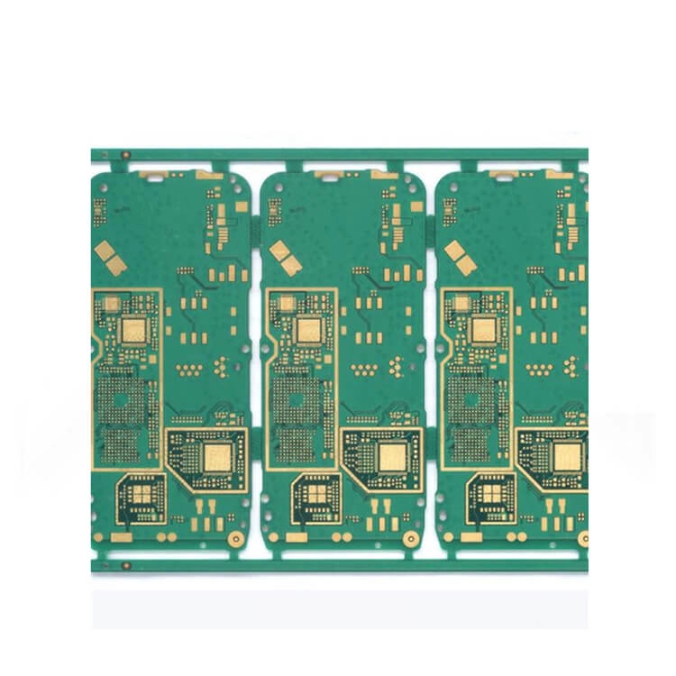
There are conductive patterns on both sides of the insulating substrate, generally using metallization holes to connect the conductive patterns on both sides cause both sides have conductive patterns, such PCBs can be used through metal holes to wrap the wiring to the other side and interleaved with each other, so it can be used on more complex circuits.

Subscribe to our weekly newsletter and receive exclusive offers on products you love!
 X
X