2. Scope of application of HNSX5S Military Point of Load DC to DC Converters (POL)
High-reliability electronic system for ground ,vehicle,radar,aviation and aerospace, etc.
|
Absolute Max. Rating |
|
|
Input voltage:4.5V~5.5V Input voltage(Transient,1s):6V Output Power:5.5W Storage temperature:-65℃~150℃ |
Mechanical Shock:1500g Lead solderable temperature:300℃(15s) Weight:12g
|
|
NO. |
Items |
Conditions (Unless other wise, -55℃≤Tc≤125℃, VIN=5V±0.15V) |
HNSX5S1R3 |
|
|
Min |
Max |
|||
|
1 |
Input voltage/V |
Low、high and room temperature |
4.5 |
5.5 |
|
2 |
Output voltage /V |
Full load,Low、high and room temperature |
0.86 |
0.94 |
|
0.96 |
1.04 |
|||
|
1.25 |
1.35 |
|||
|
3 |
Output current /A |
VIN=4.5V~5.5V |
― |
4 |
|
4 |
Output power/W |
|
0 |
5.2 |
|
5 |
Output ripple voltage/mV |
Vo=1.0V,IO=4A,BW=6MHz |
― |
30 |
|
6 |
Voltage regulation/mV |
VIN=4.5V~5.5V,Vo=1.0V,IO=4A |
― |
30 |
|
7 |
Load regulation /mV |
Vo=1.0V,IO=0→4A |
― |
30 |
|
8 |
Efficiency /% |
Vo=1.0V,IO=4A |
70 |
― |
|
9 |
Insulation resistance /MΩ |
TA=25℃,impose 500V DC voltage between case and any pin |
500 |
― |
|
10 |
Inhibit off voltage /V |
Vo=1.0V,IO=4A |
0 |
0.8 |
|
11 |
Inhibit on voltage /V |
Vo=1.0V,IO=4A |
2.4 |
- |
|
12 |
Inhibit current/mA |
TA=25℃,Vo=1.0V,IO=4A,Inhibit connect ground |
- |
10 |
|
13 |
Protection function/s |
TA=25℃,Vo=1.0V |
- |
2 |
|
14 |
Undervoltage open voltage/V |
TA=25℃,Vo=1.0V,IO=4A |
2.4 |
4.3 |
|
15 |
Undervoltage shutdown voltage/V |
TA=25℃,Vo=1.0V,IO=4A |
2.2 |
3.7 |
|
16 |
Input surge voltage/V |
Vo=1.0V,IO=4A |
- |
6 |
|
17 |
Vo=1.0V,IO=4A,no effect on DC parameters |
― |
1000 |
|
|
18 |
Vo=1.0V,IO=4A |
600 |
750 |
|
|
19 |
Step Load Response Transient(Peak)/mV |
Vo=1.0V,IO=2A→4A或IO=4A→2A |
― |
300 |
|
20 |
Step Load Response Recovery /μs |
Vo=1.0V,IO=2A→4A或IO=4A→2A |
― |
200 |
|
21 |
Start-up Overshoot(peak)/mV |
Input voltageVIN:0→5V,Vo=1.0V,IO=4A |
― |
50 |
|
22 |
Start-up Delay /ms |
Input voltage VIN:0→5V,Vo=1.0V,IO=4A |
― |
5 |


Fig 4 HNSX5S1R3 Load

Fig 5 HNSX5S1R3 Overshoot/Start-up Delay


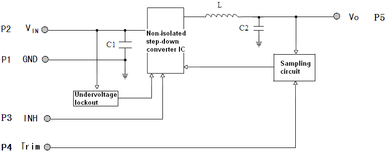
Table 4 Pin Designation
|
Pin |
Symbol |
Designation |
|
1 |
GND |
Common ground |
|
2 |
VIN |
Input |
|
3 |
INH |
Inhibit |
|
4 |
Trim |
Output trimming |
|
5 |
Vo |
Output |


|
Vo(V) |
Rtr(kΩ) |
|
1.3 |
20.3 |
|
1.2 |
27.7 |
|
1.1 |
42.5 |
|
1.0 |
87.1 |
|
0.9 |
None |

Fig 9 High level inhibit drive circuit

|
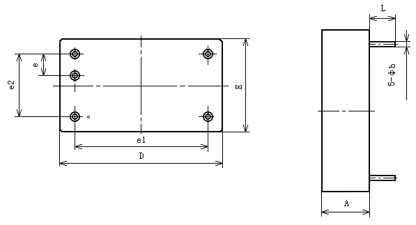
Symbols |
Unit/mm |
||
|
Minimum |
Nominal |
Maximum |
|
|
A |
- |
- |
8.50 |
|
фb |
0.87 |
1.00 |
1.13 |
|
D |
- |
- |
22.50 |
|
E |
- |
- |
15.50 |
|
e |
2.88 |
3.18 |
3.48 |
|
e1 |
15.58 |
15.88 |
16.18 |
|
e2 |
9.22 |
9.52 |
9.82 |
|
L |
5.20 |
- |
- |
|
Case Model |
Header |
Header Plating |
Cover |
Cover Plating |
Pin |
Pin Plating |
Sealing |
Notes |
|
UPP2215-05 |
Cold Rolled Steel (10#) |
Ni |
Kovar(4J42) |
Ni |
Copper –core Compound |
Au |
Parallel seam welding |
|


 X
X