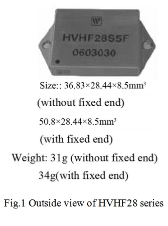
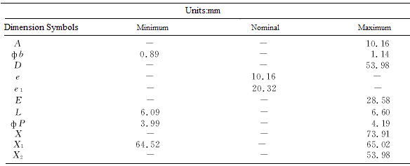
Table 1 Product models
|
MODELS |
||
|
SINGLE |
DUAL |
TRIPLE |
|
HTR28S5(F) |
HTR28D5(F) |
HTR28T512(F) |
|
HTR28S12(F) |
HTR28D12(F) |
HTR28T515(F) |
|
HTR28S15(F) |
HTR28D15(F) |
HTR28T515-A |
|
HTR28S3R3 |
|
HTR28T515-B |
|
HTR28S18(F) |
|
|
| Single output models | HTR28S5(F) | HTR28S12(F) | HTR28S15(F) | |||||
| Parameter | Conditions | Min | Max | Min | Max | Min | Max | |
| Output Voltage(V) | Io=full | Ambient temperature | 4.95 | 5.05 | 11.88 | 12.12 | 14.85 | 15.15 |
| load | high and low temperature | 4.85 | 5.15 | 11.64 | 12.36 | 14.55 | 15.45 | |
| Output Current(A) | Vin = 16 TO 40 VDC | — | 5 | — | 2.5 | — | 2 | |
| Output Power(W) | — | — | 25 | — | 30 | — | 30 | |
|
Output Ripple Voltage (mV) |
BW=10 kHz to 2 MHz Io=full load |
Ambient temperature | — | 50 | — | 40 | — | 40 |
| high and low temperature | — | 90 | — | 90 | — | 90 | ||
|
Line Regulation (mV) |
Vin = 16 TO 40 VDC, Io=full load |
— | 50 | — | 50 | — | 50 | |
|
Load Regulation (mV) |
Io=No load to load | — | 50 | — | 50 | — | 50 | |
|
Input Ripple Current (mA) |
BW=10 kHz to 10 MHz Io=full load |
— | 50 | — | 50 | — | 50 | |
|
Efficiency (%) |
Io=full load | Ambient temperature | 76 | — | 80 | — | 80 | — |
| high and low temperature | 73 | — | 77 | — | 78 | — | ||
|
Isolation (MΩ) |
Input to output or any pin to case (except pin7,8) at 500 VDC, TA = 25° C |
100 | — | 100 | — | 100 | — | |
| Inhibit Function | TA = 25° C,Inhibit voltage, output disabled | yes | yes | yes | ||||
| Protection Function | TA = 25° C | yes | yes | yes | ||||
| Start-up Overshoot (mV pk) | Vin=0 to 28V, Io=full load | — | 50 | — | 120 | — | 150 | |
|
Start-up Delay (ms) |
Vin=0 to 28V, Io=full load | — | 5 | — | 5 | — | 5 | |
|
Capacitive Load (μF) |
TA = 25° C, No effect on DC performance | — | 300 | — | 3000 | — | 3000 | |
|
Switching Frequency(kHz) |
Io=full load |
400 |
600 |
400 |
600 |
400 |
600 |
|
Step Load Response Transient (mV pK) |
50% load -- full load -50% load |
-300 |
300 |
-400 |
400 |
-500 |
500 |
|
Step Load Response Recovery (µs) |
50% load -- full load -50% load |
— |
200 |
— |
200 |
— |
200 |
|
Step Line Response Transient (mV pK) |
Vin=16~40V, Io=full load Vin=40~16V, Io=full load |
-300 |
300 |
-500 |
500 |
-600 |
600 |
|
Step Line Response Recovery (µs ) |
Vin=16~40V, Io=full load Vin=40~16V, Io=full load |
— |
300 |
— |
300 |
— |
300 |
|
Load Fault Short Circuit recovery (ms) |
short circuit to full load |
— |
5 |
— |
5 |
— |
5 |
| Single output models | HTR28S3R3 | HTR28S18 | ||||
| Parameter | Conditions | Min | Max | Min | Max | |
| Output Voltage | Io=full | Ambient temperature | 3.267 | 3.333 | 17.82 | 18.18 |
| (V) | load | high and low temperature | 3.201 | 3.399 | 17.46 | 18.54 |
| Output Current(A) | Vin= 16 TO 40 VDC | — | 6.06 | — | 1.67 | |
| Output Power(W) | — | — | 20 | — | 30 | |
| Output Ripple Voltage | BW=10kHzto 2 MHz | Ambient temperature | — | 40 | — | 40 |
| (mV) | Io=full load | |||||
| high and low temperature | — | 50 | — | 90 | ||
| Line Regulation(mV) | Vin = 16 TO 40 VDC,Io=full load | — | 10 | — | 50 | |
| Load Regulation(mV) | Io=No load to load | — | 10 | — | 50 | |
| Input Ripple Current(mA) | BW=10 kHz to 10 MHz, Io=full load | — | 50 | — | 50 | |
| Efficiency (%) | Io=full load | Ambient temperature | 74 | — | 81 | — |
| high and low temperature | 71 | — | 78 | — | ||
| Isolation (MΩ) | Input to output or any pin to case (except pin7,8) at 500 VDC, TA = 25°C | 100 | — | 100 | — | |
| Inhibit Function | TA = 25°C,Inhibit voltage, output disabled | yes | yes | |||
| Protection Function | TA = 25°C | yes | yes | |||
| Start-up Overshoot (mV pk) | Vin=0 to 28V, Io=full load | — | 50 | — | 180 | |
| Start-up Delay(ms) | Vin=0 to 28V, Io=full load | — | 5 | — | 5 | |
| Capacitive Load(μF) | TA = 25°C, No effect on DC performance | — | 300 | — | 2000 | |
| Switching Frequency(kHz) | Io=full load | 400 | 600 | 400 | 600 | |
| Step Load Response Transient (mV pK) | 50% load -- full load -50% load | -250 | 250 | -600 | 600 | |
| Step Load Response | 50% load -- full load -50% load | — | 200 | — | 200 | |
| Recovery (µs) | ||||||
| Step Line Response Transient (mV pK) | Vin=16~40V, Io=full load, | -300 | 300 | -800 | 800 | |
| Vin=40~16V, Io=full load | ||||||
| Step Line Response | Vin=16~40V, Io=full load, | — | 300 | — | 300 | |
| Recovery (µs ) | Vin=40~16V, Io=full load | |||||
| Load Fault Short Circuit recovery (ms) | short circuit to full load | — | 5 | — | 5 | |
| Dual output models | HTR28D5(F) | HTR28D12(F) | HTR28D15(F) | |||||||
| Parameter | Conditions | Min | Max | Min | Max | Min | Max | |||
|
Output Voltage (V) |
Io1=Io2=full load |
Ambient temperature | 4.95 | 5.05 | 11.88 | 12.12 | 14.85 | 15.15 | ||
| high and low temperature | 4.85 | 5.15 | 11.64 | 12.96 | 14.55 | 15.45 | ||||
| Ambient temperature | -5.075 | -4.925 | -12.18 | -11.82 | -15.23 | -14.77 | ||||
| high and low temperature | -5.172 | -4.825 | -12.42 | -11.58 | -15.53 | -14.47 | ||||
| Output Current(A) | VIN = 16 TO 40 VDC | — | 2.5 | — | 1.25 | — | 1 | |||
|
Output Power (W) |
— | — | 25 | — | 30 | — | 30 | |||
|
Output Ripple Voltage (mV) |
BW=10 kHz to 2 MHz Io1= Io2= full load |
Ambient temperature | — | 40 | — | 80 | — | 80 | ||
| high and low temperature | — | 90 | — | 120 | — | 120 | ||||
| Ambient temperature | — | 40 | — | 80 | — | 80 | ||||
| high and low temperature | — | 90 | — | 120 | — | 120 | ||||
|
Line Regulation (mV) |
VIN = 16 TO 40 VDC, Io1= Io2= full load |
+Vout | — | 50 | — | 50 | — | 50 | ||
| -Vout | — | 100 | — | 150 | — | 180 | ||||
|
Load Regulation (mV) |
Io1= Io2=No load to full load | +Vout | — | 50 | — | 50 | — | 50 | ||
| -Vout | — | 100 | — | 150 | — | 180 | ||||
| Input Ripple current (mA) |
BW=10 kHz to 10 MHz Io1= Io2= full load |
— | 50 | — | 50 | — | 50 | |||
|
Efficiency (%) |
Io1= Io2=full load | Ambient temperature | 76 | — | 79 | — | 80 | — | ||
| high and low temperature | 73 | — | 76 | — | 77 | — | ||||
|
Isolation (MΩ) |
Input to output or any pin to case (except case ground pin) at 500 VDC, TA = 25° C | 100 | — | 100 | — | 100 | — | |||
|
Inhibit Function Protection Function |
TA = 25° C,Inhibit voltage, output disabled TA = 25° C |
yes | yes | yes | ||||||
| yes | yes | yes | ||||||||
| Start-up Overshoot (mV pk) | Vin=0 to 28V, Io1=Io2=full load | -180 | 180 | -120 | 120 | -150 | 150 | |||
|
Start-up Delay (ms) |
Vin=0 to28V, Io1=Io2=full load | — | 5 | — | 5 | — | 5 | |||
| Capacitive Load(μF) | TA = 25° C, No effect on DC performance | — | 500 | — | 500 | — | 500 | |||
|
Switching Frequency (kHz) |
Io=full load | 400 | 600 | 400 | 600 | 400 | 600 | |||
|
Step Load Response Transient (mV pK) |
50% load to full load or full load to 50% load | -300 | 300 | -300 | 300 | -400 | 400 | |||
|
Step Load Response Recovery (µs) |
50% load to full load or full load to 50% load, |
— |
200 |
— |
200 |
— |
200 |
|
Step Line Response Transient (mV pK) |
Vin=16~40V, Io1= Io2=full load Vin=40~16V, Io1= Io2=full load
|
-400 |
400 |
-400 |
400 |
-500 |
500 |
|
Step Line Response Recovery (µs ) |
Vin=16~40V, Io1= Io2=full load Vin=40~16V, Io1= Io2=full load |
— |
300 |
— |
300 |
— |
300 |
|
Load Fault Short Circuit recovery (ms) |
Io1= Io2 : short circuit to full load |
— |
5 |
— |
5 |
— |
5 |
| Triple output models | HTR28T512(F) | HTR28T515(F) | ||||
| Parameter | Conditions | Min | Max | Min | Max | |
|
Output Voltage (V) |
Io1= Io2= Io3 =full load | Ambient temperature | 4.95 | 5.05 | 4.95 | 5.05 |
| high and low temperature | 4.85 | 5.15 | 4.85 | 5.15 | ||
| Ambient temperature | 11.82 | 12.18 | 14.77 | 15.23 | ||
| high and low temperature | 11.58 | 12.42 | 14.47 | 15.52 | ||
| Ambient temperature | -12.18 | -11.82 | -15.23 | -14.77 | ||
| high and low temperature | -12.42 | -11.58 | -15.52 | -14.47 | ||
|
Output Current (A) |
VIN = 16 TO 40 VDC | +5Vout | 0.1 | 4 | 0.1 | 4 |
| +Vout | — | 0.416 | — | 0.333 | ||
| -Vout | — | 0.416 | — | 0.333 | ||
|
Output Power (W) |
— | — | 30.84 | — | 30.84 | |
| Output Ripple Voltage(mV) |
BW=10 kHz to 2 MHz Io1= Io2= Io3 = full load |
+5Vout | — | 125 | — | 125 |
| +Vout | -60 | 60 | -60 | 60 | ||
| -Vout | -60 | 60 | -60 | 60 | ||
|
Line Regulation (mV) |
VIN = 16 TO 40 VDC, Io1= Io2= Io3 = full load |
+5Vout | — | 20 | — | 20 |
| +Vout | -75 | 75 | -75 | 75 | ||
| -Vout | -75 | 75 | -75 | 75 | ||
|
Load Regulation (mV) |
Io1= Io2= Io3 =No load to full load | +5Vout | — | 50 | — | 50 |
| +Vout | -75 | 75 | -75 | 75 | ||
| -Vout | -75 | 75 | -75 | 75 | ||
| Input Ripple current (mA) | BW=10 kHz to 10 MHz | Ambient temperature | — | 45 | — | 45 |
| Io= full load | high and low temperature | — | 80 | — | 80 | |
| Efficiency (%) | Io1= Io2= Io3=full load | Ambient temperature | 72 | — | 73 | — |
| high and low temperature | 70 | — | 71 | — | ||
| Isolation (MΩ) | Input to output or any pin to case (except pin 6,7) at 500 VDC, TA = 25° C | 100 | — | 100 | — | |||
| Inhibit Function | TA = 25° C,Inhibit voltage, output disabled | yes | yes | |||||
| Protection Function | TA = 25° C | yes | yes | |||||
| Start-up Overshoot (mV pk) | Vin=0 to 28V, Io =full load | +5Vout | — | 500 | — | 500 | ||
| +Vout | — | 1500 | — | 1500 | ||||
| -Vout | — | 1500 | — | 1500 | ||||
| Start-up Delay(ms) | Vin=0 to28V, Io =full load | — | 6 | — | 6 | |||
| Capacitive Load(μF) | TA = 25° C, No effect on DC performance | — | — | — | — | |||
| Switching Frequency(kHz) | Io=full load | 400 | 600 | 400 | 600 | |||
| Step Load Response Transient (mV pK) | 50% load to full load or full load to 50% load, | +5Vout | -250 | 250 | -250 | 250 | ||
| +Vout | -800 | 800 | -800 | 800 | ||||
| -Vout | -800 | 800 | -800 | 800 | ||||
| Step Load Response Recovery (mV pK) | 50% load to full load or full load to 50% load, | +5Vout | — | 100 | — | 100 | ||
| +Vout | — | 4000 | — | 4000 | ||||
| -Vout | — | 4000 | — | 4000 | ||||
| Step line Response Transient (mV pK) |
Vin=16~40V, Io =full load Vin=40~16V, Io =full load |
-800 | 800 | -800 | 800 | |||
| Step Line Response |
Vin=16~40V, Io =full load Vin=40~16V, Io =full load |
— | 5000 | — | 5000 | |||
| Recovery (µs ) | ||||||||
| Load Fault recovery (ms) | Io :short circuit to full load | — | 6 | — | 6 | |||
| Parameter | Conditions | Min | Max | Min | Max | |
|
Output Voltage (V) |
Io1= Io2= Io3 =full load | Ambient temperature | 4.9 | 5.1 | 4.9 | 5.1 |
| high and low temperature | 4.8 | 5.2 | 4.8 | 5.2 | ||
| Ambient temperature | -15.15 | -14.85 | -15.15 | -14.85 | ||
| high and low temperature | -15.4 | -14.6 | -15.4 | -14.6 | ||
| Ambient temperature | 14.85 | 15.15 | 14.85 | 15.15 | ||
| high and low temperature | 14.6 | 15.4 | 14.6 | 15.4 | ||
|
Output Current (A) |
VIN = 16 TO 40 VDC | +5Vout | 3 | — | 3 | — |
| +Vout | 0.5 | — | 0.5 | — | ||
| -Vout | 0.5 | — | 0.5 | — | ||
| Output Power(W) | — | — | 30.84 | — | 30.84 | |
|
Output Ripple Voltage (mV) |
BW=10 kHz to 2 MHz Io1= Io2= Io3 = full load |
+5Vout | — | 50 | — | 80 |
| +Vout | — | 100 | — | 100 | ||
| -Vout | — | 100 | — | 100 | ||
|
Line Regulation (mV) |
VIN = 16 TO 40 VDC, Io1= Io2= Io3 = full load |
+5Vout | — | 50 | — | 50 |
| +Vout | — | 80 | — | 80 | ||
| -Vout | — | 80 | — | 80 | ||
|
Load Regulation (mV) |
Io1= Io2= Io3 =No load to full load | +5Vout | — | 50 | — | 50 |
| +Vout | — | 80 | — | 100 | ||
| -Vout | — | 80 | — | 100 | ||
|
Input Ripple current (mA) Efficiency (%) |
BW=10 kHz to 10 MHz Io= full load Io1= Io2= Io3=full load |
— | — | — | — | |
| 75 | — | 75 | — | |||
|
Isolation (MΩ) |
Input to output or any pin to case (except pin 6,7) at 500 VDC, TA = 25° C | 100 | — | 100 | — | |
| Inhibit Function |
TA = 25° C,Inhibit voltage, output disabled TA = 25° C |
yes | yes | |||
| Protection Function | — | — | ||||
| Start-up Overshoot (mV pk) | Vin=0 to 28V, Io =full load | +5Vout | — | — | — | — |
| +Vout | ||||||
| -Vout | ||||||
|
Start-up Delay(ms) Capacitive Load(μF) |
Vin=0 to28V, Io =full load TA = 25° C, No effect on DC performance |
— | — | — | — | |
| — | — | — | — | |||
| Switching Frequency(kHz) | Io=full load | — | — | — | — | |
| Step Load Response Transient (mV pK) | 50% load to full load or full load to 50% load, | +5Vout | — | — | — | — |
| +Vout | ||||||
| -Vout | ||||||
| Step Load Response Recovery (mV pK) | 50% load to full load or full load to 50% load, | +5Vout | — | — | — | — |
| +Vout | ||||||
| -Vout | ||||||
| Step line Response Transient (mV pK) |
Vin=16~40V, Io =full load Vin=40~16V, Io =full load |
— | — | — | — | |
|
Step Line Response Recovery (µs ) |
Vin=16~40V, Io =full load Vin=40~16V, Io =full load |
— | — | — | — | |
| Load Fault recovery (ms) | Io :short circuit to full load | — | — | — | — | |
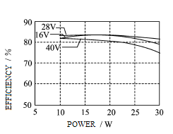
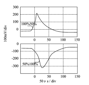
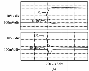
4 TYPICAL PERFORMANCE CURVES
(1)Single output (Model HTR28S15)
 |
 |
|
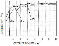
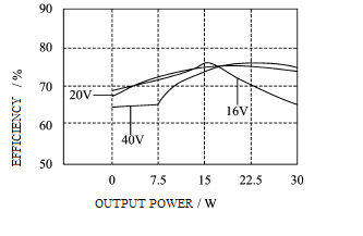
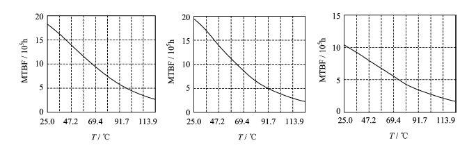
Figure 2 Efficiency (Output Power) |
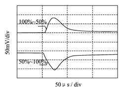
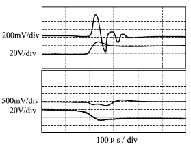
Figure 3 Step Load Response |
 |
 |
|
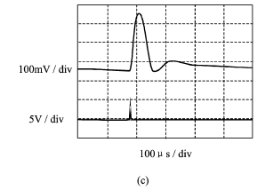
Figure 4 Step Line response |
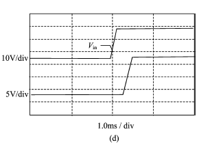
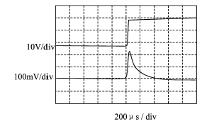
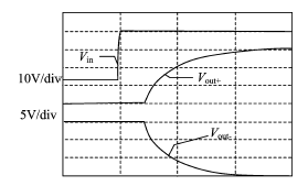
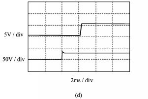
Figure 5 Start-up Overshoot/ Start-up Delay |
 |
 |
|
Figure 6 Efficiency (Output Power) |
Figure 7 Step Line response |
 |
 |
|
Figure 8 Step Load Response |
Figure 11 Step Line response |
 |
 |
|
Figure 10 Efficiency (Output Power) |
Figure 11 Step Line response |
 |
 |
|
Figure12 Step Load Response |
Figure13 Start-up Overshoot/ Start-up Delay |
|
|
|
|
|
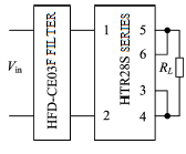
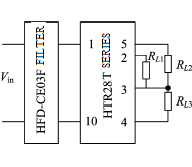
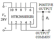
Figure 17 Application Connection Diagram for Single output models |
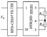
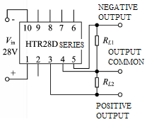
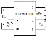
Figure 18 Application Connection Diagram for Dual output models |
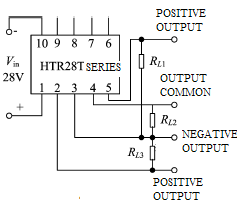
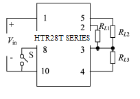
Figure 19 Application Connection Diagram for Triple output models |
|
|
|
|
|
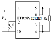
Figure 20 Inhibit Drive connection Diagram for Single Output Models |
Figure21 Inhibit Drive connection Diagram for Dual Output Models |
Figure 22 Inhibit Drive connection Diagram for Triple Output Models |
 |
 |
 |
|
Figure23 Single Output Converter with EMI Filter connection Diagram |
Figure24 Dual Output Converter with EMI Filter connection Diagram |
Figure25 Triple Output Converter with EMI Filter connection Diagram |
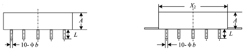
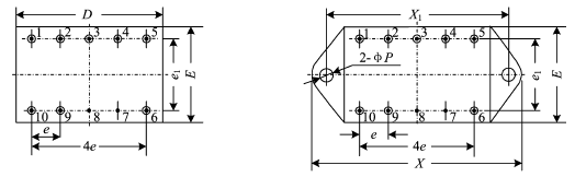 Bottom View Bottom View |
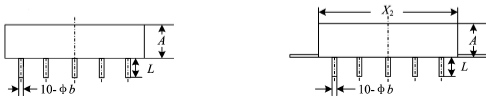 Side View Side View |
|
Figure 26 Single Output Model |
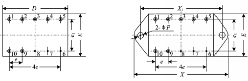 Bottom View Bottom View |
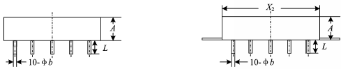 Side View Side View |
|
Figure 27 Dual Output Model |
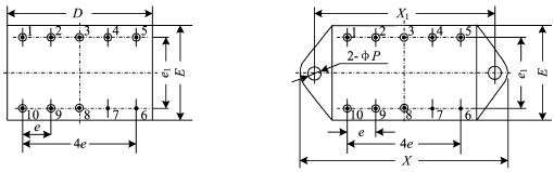 Bottom View Bottom View |
 Side View Side View |
|
Figure 28 Triple Output Model |
|
Case Model |
Header |
Header Plating |
Cover |
Cover Plating |
Pin |
Pin Plating |
Sealing Style |
Notes |
|
UPP5429-10 (Single&Dual ) |
Cold Rolled Steel(10#) |
Nickel |
Iron/Nickel Alloy(4J42) |
Nickel |
Copper Compound |
Nickel/Gold |
Compression Seal |
Nickel plating is for case ground pin. |
|
UPP5034-10c (Triple ) |
Cold Rolled Steel(10# |
Nickel |
Iron/Nickel Alloy(4J42) |
Nickel |
Iron/Nickel Alloy(4J50) |
Nickel/Gold |
Compression Seal |
Nickel plating is for case ground pin. |
 |
||
|
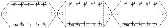
Figure29 Pin Out Bottom View (Single) |
Figure29 Pin Out Bottom View (Dual) |
Figure29 Pin Out Bottom View (Triple) |
|
Pin |
Single Output |
Dual Output |
Triple Output |
|
1 |
Positive Input |
Positive Input |
Positive Input |
|
2 |
Inhibit |
Inhibit |
Positive Output (5V) |
|
3 |
Negative Inductive |
Positive Output |
Output Common |
|
4 |
Output Common |
Output Common |
Negative Output |
|
5 |
Positive Output |
Negative Output |
Positive Output |
|
6 |
Positive Inductive |
Case Ground |
Case Ground |

Subscribe to our weekly newsletter and receive exclusive offers on products you love!
 X
X


 Gold Supplier