Product Detail
Synchro/Resolver-Digital Converter
(HSDC/HRDC174 Series)
1. Product characteristics (see Fig. 1 for outside view, and Table 1 for models)
Internal differential isolation conversion
Resolution: 12 bits, 14 bits
Three-state latch output
High continuous tracking speed
32-wire salt fog metal case package
MCM high-density assembly
Antistatic capacity 2000V
Pin-to-pin compatible with SDC/RDCl740/1741/1742 product of AD company
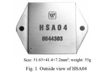
Size: 44.2×28.9×7.2mm3; weight: 22g
Fig. 1 Outside view of HSDC/HRDC174 Series
2. Scope of application
Flight instrument system;
Artillery control system;
Avionics control system;
Radar control system;
Ship navigation system;
Antenna monitoring system;
Robot system;
CNC lathe;
Other various automatic control system Table 1 product models
12-bit 14-bit
Synchro Resolver Synchro Resolver
HSDCl742-X11 HRDCl742-X13 HSDCl744-X11 HRDCl744-X13
HSDCl742-X12 HRDCl742-X14 HSDCl744-X12 HRDCl744-X14
HSDCl742-X41 HRDCl742-X18 HSDCl744-X41 HRDCl744-X18
HSDCl742-X42 HRDCl742-X23 HSDCl744-X42 HRDCl744-X23
HSDCl742-X21 HRDCl742-X24 HSDCl744-X21 HRDCl744-X24
HSDCl742-X22 HRDCl742-X28 HSDCl744-X22 HRDCl744-X28
HRDCl742-X43 HRDCl744-X43
HRDCl742-X44 HRDCl744-X44
HRDCl742-X48 HRDCl744-X48
3. Outline
HSDC/HDC174 series products are hybrid integrated 12-bit or 14-bit continuous tracking synchro/resolver to digital converter designed according to type II servo principle. This series products adopt MCM process, the core elements adopt special chips developed independently by our institute. The product adopts 32-wire DIL shallow cavity salt spray resistant metal case package with small volume and light weight, and pin-to-pin compatible with SDC/RDC1740/1741/1742 products of AD company, USA.
The design and manufacture of HSDC/HRDCl74 meet the requirements of GJB 2438A-2002 “General Specification for Hybrid Integrated Circuits” and product specification with quality assurance grade of H. 4. Technical performance (Table 2, Table 3)
Table 2 Rated conditions and recommended operating conditions
Max. absolute rating value Supply voltage Vs: ± 17.25VDC
Logical supply voltage VL: +7V
Storage temperature range: -65℃~+150℃
Recommended operating conditions Supply voltage Vs: ±15±0.75V
5V power voltage: 5±0.25V
Effective value of reference voltage VRef: 115V, 26V, 11.8V
Effective value of signal voltage V1: 90V, 26V, 11.8V
Reference frequency f*: 400Hz, 50Hz, 2.6kHz
Range of operating temperature TA: -55℃~125℃
Note: * indicates it can be customized as per user’s requirement.
Table 3 Electric characteristics (-55~+125℃)
Characteristics HSDC/HRDC1740 series HSDC/HRDC1744 series Unit Remarks
Accuracy ±8.5 (max.) ±5.3 (max.) Angular minute
Tracking speed 36 (typical) 27 (typical) r/sec
Resolution 12 14 Bit
Signal and reference frequency 50~2600 50~2600 Hz
Signal input voltage 2~90 2~90 V
Reference input voltage 2~115 2~115 V
Signal input impedance 90V Single-end 100 100 kΩ
Signal Differential 200 200 kΩ
26V Single-end 28 28 kΩ
Signal Differential 56 56 kΩ
11.8V Single-end 13 13 kΩ
Signal Differential 26 26 kΩ
Reference input impedance 115V Single-end 127 127 kΩ
Reference Differential 254 254 kΩ
26V Single-end 28 28 kΩ
Reference Differential 56 56 kΩ
90V Single-end 100 100 kΩ
Reference Differential 200 200 kΩ
Acceleration constant 80000 (min.) 56000 (min.) s2 Design guarantee
Step response 75 (max.) 100 (max.) ms
Supply current +VS +15V 35 (max.) 35 (max.) mA
-VS +15V 35 (max.) 35 (max.) mA
VL +5V 56 (max.) 56 (max.) mA
Power consumption 1.4 (max.) 1.4 (max.) W
Settling or release time 80 (max.) 80 (max.) ns
Settling time 640 (max.) 640 (max.) ns
Busy pulse width 200~600 (typical 400) 200~600 (typical 400) ns
Loading capacity 2 (min.) 2 (min.) TTL
Digital output VOH 3.3 (min.) 3.3 (min.) VDC
VOL 0.7 (max.) 0.7 (max.) VDC
Loading capacity 3 (max.) 3 (max.) TTL
Selection of operating temperature range 8YZ -55~+125 -55~+125 ℃
5. Operating principle (Fig. 2 and Fig. 3)
The input signal of synchro (or resolver) is converted into the orthogonal signal through the internal differential isolation:
Vsin=KE0sin(ωt+α) sinθ (sin)
Vcos=KE0sin(ωt+α) cosθ (cos)
Where, θ is the analog input angle.
These two signals and the digital angle φ of internal reversible counter are multiplied in the multiplier of sine and cosine functions and error signal is obtained after processing:
KE0sin(ωt+α) (sinθ cosφ -cosθ sinφ)
i.e. KE0sin(ωt+α) sin(θ-φ)
This signal is sent to voltage-controlled oscillator after amplification, phase discrimination, integration filtration. If θ-φ≠0, voltage controlled oscillator will output pulses and the reversible counter counts them until θ-φ=0. In this process, the converter tracks the change of input angle all the time.
Fig.2 Block diagram for operating principle
Fig. 3 Time sequence diagram for bus transfer
logic input only inhibits data transfer from reversible counter to output latch without interrupting the operation of the tracking loop. When Inhibit system is released, a pulse will be generated automatically, which is used to update output data.
input determines the status of output data. Whereas Logic Hi makes output end appear in high impedance status; Logic Low transfers the data in latch to the output pins. starts the high 8-bit data to be valid, whereas starts the low 6-bit data to be valid (HSDC/HRDC1742 is of low 4-bit type).
Busy
When the input of the converter changes, Busy outputs a train of pulses of CMOS level, its frequency is determined by the highest rotational speed. The falling edge of Busy pulses triggers the latch to update the data and the output data is valid after max. 600ns delay. The typical width of Busy pulses is 400ns. The load capacity of the output is 3TTL.
(1) Methods and time sequence of data transfer
Following two methods are available for data transfer:
① mode
After 640ns of logic low, the output data is valid, and the converter realizes data transfer through and . After Inhibit is released, the system will automatically generate a pulse with its width equal to that of Busy pulse for data updating.
② Bust mode:
At the rising edge of Busy pulse, the three-state reversible counter counts; at the descending edge of Busy pulse, it internally generates a latch pulse with its width equal to that of Busy pulse for updating the data of the three-state latch, the time sequence of data transfer is shown in Fig.3, in other words, after 600ns of Busy logic low, the stable transfer of data is valid. In asynchronous reading mode, Busy output is a pulse train of CMOS level, the widths of its high and low level depend on operating frequency and rotating speed of the device selected.
(2) Compatibility
When HSDC/HRDC174 series products are used under the condition of non-nominal signals and non-nominal reference voltage, proportional resistances are connected in series at the signal end and excitation input end of them in order to realize compatibility.
Example 1: Connection of HSDC1742-441 for excitation voltage/signal voltage/frequency of 36V/26V/400Hz is shown in Fig. 4:
Example 2: Connection of HRDC1742-418 for excitation voltage/signal voltage/frequency of 36V/26V/400Hz is shown in Fig. 5:
Fig. 4 Connection of HSDC1742-411
Fig. 5 Connection of HSDC1742-418 R1=(V1 - V1 nominal value)×1.11 k
=(26 V- 11.8 V)×1.11 k
=15.8 kΩ
R2=(VRef - VRef nominal value)×1.11 k
=(36 - 26)×1.11 k
=11.1 kΩ
R3=(V1 - V1 nominal value)×1.11 k
=(26 V- 11.8 V)×1.11 k
=15.8 kΩ
R4=(VRef - VRef nominal value)×1.11 k
=(36 - 26)×1.11 k
=11.1 kΩ
(3) Dynamic behavior
Transfer function of the converter is given by Fig. 6:
Closed-loop gain:
Closed-loop gain:
θin + θout
Fig. 6 Transfer function
Model: HSDC/HRDC1742
Here, Ka=80000, T1=0.0087, T2=0.001569
(4) Acceleration error
The converter is designed using the tracking principle of type II servo loop, so theoretically speaking, it does not have speed lag error, but has acceleration error. This error can be defined as follows using acceleration constant K of the converter:
Ka=
Below is the example for calculating the tracking error of the 14-bit converter HSDC1744 using the acceleration constant Ka:
Ka=56000, the acceleration is 50 revolutions/s2
Error of least significant bit = =14.62LSBs
6. Typical characteristic curves (Fig. 7 and Fig. 8)
Frequency/Hz
Fig. 7 Gain chart of HSDC/HRDC1742
Frequency/Hz
Fig. 8 Gain chart of HSDC/HRDC1742
7. MTBF curve (Fig. 9)
Temperature/℃
Fig. 9 MTBF-temperature curve 8. Pin designation (Fig. 10, Table 4)
Fig. 10 Pins (Bottom view)
(Note: according to GJB/Z299B-98, envisaged good ground condition)
Table 4 Pin designation
Pin Symbol Function Pin Symbol Function
1 D1 Digital output 1 (MSB) 17② NC/S4 No connection/resolver input S4
2 D2 Digital output 2 18 S3 Resolver/synchro input S3
3 D3 Digital output 3 19 S2 Resolver/synchro input S2
4 D4 Digital output 4 20 S1 Resolver/synchro input S1
5 D5 Digital output 5 21 NC No connection
6 D6 Digital output 6 22 NC No connection
7 D7 Digital output 7 23 Case Case
8 D8 Digital output 8 24④ NC或(Vel)* No connection (or speed output)
9 D9 Digital output 9 25③ Enable low 4-bit/6-bit
10 D10 Digital output 10 26 Enable high 8-bit
11 D11 Digital output 11 27 Busy “Busy” signal
12 D12 Digital output 12 28 Inhibit
13 NC/D13 No connection/digital output 13 29 +VS +15V power
14 NC/D14 No connection/digital output 14 30 GND Ground
15 RLo Low end of reference signal input 31 -VS -15V power
16 RHi High end of reference signal input 32 VLo +5V power
Notes: ① For HSDC1742 and HRDC1742 series converters, pin 13 and 14 are not connected;
② For HSDC174X, pin 17 is not connected; for HRDC174X, pin 17 is input end of resolver S4;
③ For HSDC1742 and HRDC1742 series converters, pin 25 is for Enable low 4-bit control;
④ When there is speed requirement, it is led out from pin 24.
9. Table of weight values (Table 5)
Table 5 Table of weight values
Bit Angle Bit Angle Bit Angle
1 180.0000 6 5.6250 11 0.1758
2 90.0000 7 2.8125 12 (for 12-bit LSB) 0.0879
3 45.0000 8 1.4063 13 0.0439
4 22.5000 9 0.7031 14 (for 14-bit LSB) 0.0220
5 11.2500 10 0.3516
10. Connection diagram for typical application (Fig. 11)
Notes:
(1) The voltage across pin 29 and pin 31 should be ±15 V, and should not be connected reversely. Digital logic power +5V is connected to pin 32.
(2) Between the power supply and ground, 0.1µF ceramic capacitor and 6.8µF electrolytic capacitor shall be connected in parallel.
(3) The pin marked with Case has been connected to the case.
(4) Digital outputs of HSDC/HRDC1742 are pin 1 to 12, pin 13 and 14 are not connected.
Fig. 11 Connection diagram for typical application
(5) Reference is connected to RLo on pin 15 and RHi on pin 16. In the case of synchro, signals are connected to S1, S2, and S3 as per the following conventions:
sin(ωt+α) sinθ
sin(ωt+α) sin(θ+120o)
sin(ωt+α) sin(θ+240o)
In the case of resolver, signals are connected to S1, S2, S3 and S4 as per the following conventions:
sin(ωt+α) sinθ
sin(ωt+α) cosθ
(6) For resolver, pin 17 is S4, and for synchro, pin 17 is not connected.
11. Package specifications (unit: mm) (Fig. 12, Table 6 and 7)
Fig.8 Outside view of package Table 6 Symbols and nominal values
Symbol Nominal value
A 7.2
Φb 0.45
D 44.2
E 28.9
e 2.54
e1 22.86
L 5min
Table 7 Case materials
Case model Header Header plating Cover Cover plating Pin material Pin plating Sealing style Remarks
UP4429- 32a Kovar (4J29) Ni Fe-Ni alloy (4J42) Ni Kovar (4J29) Ni/Au Matched packaging Coating of pin 23 is Ni
Note: temperature of the solder pins shall not exceed 300℃ within 10s.
12. Part numbering key (Fig. 13)
Fig. 13 Part numbering key
Note: when the above signal voltage and reference voltage (Z) are non-standard, they shall be given as follows:
(e.g. reference voltage 5V and signal voltage 3V are expressed as -5/3)
Precautions for use
Supply voltage must be kept to the voltage of correct polarity.
When the max. absolute rated value is exceeded, the device may be damaged.
During the assembly, the bottom of the product shall fit to the circuit board closely so as to avoid damage of pins, and shockproof provision shall be added, if necessary.
Do not bend the pinouts, otherwise this will cause breakage of the insulator, which affects the sealing property.
When the user places an order for the product, detailed electric performance indexes shall refer to the relevant enterprise standard.
Synchro/Resolver-Digital Converter
(HSDC/HRDC1746 Series)
1. Features (see Fig. 1 for outside view, and Table 1 for models)
Internal differential isolation conversion
Resolution:16 bits
Three-state latch output
Uninterrupted tracking during data transfer
32-wire metal case package
Size: 45.39×29.0×7.2mm2; Weight: 28g
Fig. 1 Outside view of HSDC/HRDC1746 Series Table 1 Product models
HRDC1746 418
HRDC1746 414
2. Scope of application
Flight instrument system; military servo control system; cannon control system; aviation electronic system; radar control system; naval vessel navigation system; antenna monitoring; robot technology, computerized numeric control (CNC) machine tools; and other automation control system.
3. Outline
HSDC/HRDC1746 series synchro/resolver--digital converter is designed on the principle of type II servo tracking principle and adopts differential isolation input, the data output adopts three-state latch mode, it is suitable for analog signal/digital signal conversion of three-wire synchro and four-wire resolver. With fast conversion speed and stable and reliable performance, this device can be widely applied in angle measurement and automatic control system.
This product is made by the thick-film hybrid integration process and is 32-wire DIP totally sealed metal package. Design and manufacturing of products shall meet the requirements of GJB2438A-2002 “General specification of hybrid integrated circuit” and detailed specifications for products.
4. Technical performance (Table 2, Table 3)
Table 2 Rated conditions and recommended operating conditions
Max. absolute rating value Supply voltage Vs: ±17.25VOC
Logical voltage VL: +7V
Storage temperature range: -55~+150℃
Recommended operating conditions Supply voltage Vs: ±15±5%
Effective value of reference voltage VRef: ±10% of nominal value
Effective value of signal voltage Vi: ±5% of nominal value
Frequency of reference signal f*: ±10% of nominal value
Phase shift between signal and excitation: <±10%
Operating temperature range TA: 40~+105℃
Table 3 Electric characteristics
Characteristics HSDC/HRDC1746 series Remarks
Min. Max.
Accuracy/angular minute 2.6 2.6
Tracking speed: rps 3 3
Resolution/bit 16
Signal and reference frequency/Hz 50 2.6k
Signal voltage (effective value)/V 2 90
Reference voltage (effective value)/V 2 115
Note: * indicates it can be customized as per user’s requirement.
5. Operating principle
The synchro input signal (or input signal of resolver) is converted into the orthogonal signal through internal differential isolation:
V1-KE0sinθ sinωt
V2-KE0cosθ sinωt
Where, θ is the simulated input angle.
The orthogonal signal is multiplied by the binary digital angle φ in the internal reversible counter in the sine-cosine function multiplier and an error function is obtained:
KE0sinθ cosφ sinωt-KE0cosθ sinφ sinωt=KE0sin(θ-φ) sinωt
Through error amplification, phase discrimination and filtration of this error function, sin(θ-φ) is obtained, when θ-φ=0 (within the accuracy of the converter), this error will make the voltage controlled oscillator output correction pulse to change the binary digital angle φ of the reversible counter so as to make the output φ value equal to the input θ within the accuracy of the converter, the system becomes stable and can track the change of input angle φ. In this way, a binary digital angle φ representing the input shaft angle θ is obtained on the reversible counter (Fig. 2).
Fig. 2 Circuit block diagram
(1) Dynamic characteristics
Transfer function of the converter is shown in Fig. 3:
Open-loop gain:
Closed-loop function:
For the module of this model Ka=48000/S2, T1=7.1ms, T2=1.25ms
Fig. 3 Function transfer of the converter
(2) Methods of data transfer and time sequence
Chip select control
This pin is the input pin of control logic, its function is to output data to the converter to realize three-state control. Low level is valid, the output data of converter occupies the data bus. When it is at high level, the data output pin of converter is in three states, the device does not occupy the bus.
Byte select
This pin is the control logic input pin, its function is to externally execute selection control on the output data of the converter in the transfer mode of 8-bit data bus or 16-bit data bus. When 16-bit data bus transfer mode is required, keep this logic pin high, the data will be transferred in the bus, the high byte output is in pin D1 to D8 (D1 is high bit) and low byte is in D9 to D16. When 8-bit data bus transfer mode is needed, the data is obtained at pin D1 to D8 (arranged from high to low), and high 8 bits and low 8 bits are obtained through two time sequences, in other words, when Byte select is logic high, high 8 bits are output and when it is logic low, low 8 bits are output.
Data locking control (Inhibit signal )
This pin is the input pin of control logic, its function is to output data externally to the converter to realize optional latching or bypass control. At high level, the output data of the converter is directly output without latching, see the time sequence diagram of the data transfer. At low level, the output data of the converter is latched, the internal loop is not interrupted, and tracking remains working all the time, but the counter doesn’t output data. When it is needed to transfer data, the converter first makes control the signal to lock the data from high to low, keeps logic low for 640ns, then set input to low (at this time the device occupies the data bus), and then obtains data through Byte select, then turn all control logics to high to refresh and latch the data so as to get ready for transferring the next data, please refer to time sequence diagrams of data transfer Fig.4 and Fig.5.
(3) Attenuation method of input signal (Fig.4 and Fig.5)
Fig4 Time sequence of 16-bit bus transfer
Fig5 Time sequence of 8-bit bus transfer
6. MTBF curve (Fig. 6)
Fig.6 MTBF-temperature curve 7. Pin designation (Fig. 7, Table 4)
Fig. 7 Pins (Bottom view)
(Note: according to GJB/Z299B-98, envisaged good ground condition)
Table 4 Pin designation
Pin Symbol Meaning Pin Symbol Meaning
1 NC No connection 17 NC Leave unconnected
2 D9 Output for digital bit 9 18 RHi Input RHi of resolver
3 D10 Output for digital bit 10 19 RLo Input RLo of Rotary resolver
4 D11 Output for digital bit 11 20 GND Ground
5 D12 Output for digital bit 12 21 -VS -15V power
6 D13 Output for digital bit 13 22 +VS +15V power
7 D14 Output for digital bit 14 23 Digital locking control
8 D15 Output for digital bit 15 24 D1 Output for digital bit 1
9 D16 Output for digital bit 16 25 D2 Output for digital bit 2
10 Chip select Enable control 26 D3 Output for digital bit 3
11 Bysel Byte select 27 D4 Output for digital bit 4
12 S4/NC① S4 input/no connection 28 D5 Output for digital bit 5
13① S3 S3 Input 29 D6 Output for digital bit 6
14① S2 S2 Input 30 D7 Output for digital bit 7
15 S1 S1 Input 31 D8 Output for digital bit 8
16 NC No connection 32 NC No connection
Note: ① For HSDC device, S4 is not used.
8. Table of weight values (Table 5)
Table 5 Table of weight values
Bit (MSB) Angle Bit (MSB) Angle Bit (MSB) Angle Bit (MSB) Angle
1 180.0000 5 11.2500 9 0.7031 13 0.0439
2 90.0000 6 5.6250 10 0.3516 14 0.0220
3 45.0000 7 2.8125 11 0.1758 15 0.0110
4 22.5000 8 1.4063 12 0.0879 16 0.0055
Connection of the converter
±15V, +5V and GND shall be connected to corresponding pins on the converter, notice that the polarities of the power supply must be correct, otherwise, the converter may be damaged. It is recommended to connect 0.1μF and 6.8μF bypass capacitance in parallel between each power supply terminal and ground.
Signal and excitation source are allowed to be connected to S1, S2, S3 and S4 and RHi and RLo end within an error of 5%.
The signal input shall match the phase of the excitation source so that they can be correctly connected with the converter, their phases are as follows:
RHi~RLo:VRsinωt
For the synchro, signal inputs are:
For S1~S3: sinθ sinωt
For S3~S2: sin(θ+120o) sinωt
For S2~S1: sin(θ+240o) sinωt
For the resolver, signal inputs are:
For S1~S3: sinθ sinωt
For S2~S4: cosθ sinωt
Note: no input signal of RHi, RLo, S1, S2, S3 and S4 is allowed to be connected to other pins for fear of damage of the device.
10. Package specifications (unit: mm) (Fig. 8, Table 6)
Fig.8 Outside view of package
Table 6 Case materials
Case model Header Header plating Cover Cover plating Pin material Pin plating Sealing style Remarks
UP4429- 32a Kovar (4J29) Ni Fe-Ni alloy (4J42) Ni Kovar (4J29) Ni/Au Matched packaging
Note: temperature of the solder pins shall not exceed 300℃ within 10s.
11. Part numbering key (Fig. 9)
Fig. 9 Part numbering key
Note: when the above signal voltage and reference voltage (Z) are non-standard, they shall be given as follows:
(e.g. reference voltage 5V and signal voltage 3V shall be expressed as -5/3)
Precautions for use
Supply power correctly, during the power-up, accurately connect the positive and negative poles of power to avoid burnout.
During the assembly, the bottom of the product shall fit to the circuit board closely so as to avoid damage of pins, and shockproof provision shall be added, if necessary.
Do not bend the pinouts to prevent the insulator from breaking, which affect the sealing property.
When the user places an order for the product, detailed electric performance indexes shall refer to the relevant enterprise standard.
Synchro/Resolver to Digital Converter
(HSDC/HRDC211 Series)
1. Features (see Fig. 1 for outside view, and Table 1 for models)
Excitation frequency: 50Hz, 400Hz, 2.6kHz
Resolution: 10-bit, 12-bit, 14-bit
High tracking rate
Non-standard input is adjustable through external resistance or adjusted in the product input end
DC voltage output directly proportional to angular velocity
Compatible with SDC1700 series of American AD company
Size: 79.4×66.7×11.8mm2
Weight: 108g
Fig. 1 Outside view of HSDC/HRDC211 Series Table 1 Product models
12-bit 14-bit
Synchro Resolver Synchro Resolver
HSDC2112-412 HRDC2112-418 HSDC2114-412 HRDC2114-418
HSDC2112-411 HRDC2112-414 HSDC2114-422 HRDC2114-414
HRDC 2112N HSDC2114-411 HRDC 2114N
2. Scope of application
Servo system; antenna system; angle measurement; simulation technology; artillery control; control of industrial machine tools
3. Outline
This series is a digital synchro/resolver to converter of modular structure with built-in solid-state SCOTT isolation converter, designed according to the principle of type II servo, and can realize continuous tracking and conversion.
The operating power is ±15V and +5V DC power. There are two types of output signal: three-line synchro and reference signal (SDC converter) or four-line resolver and reference signal (RDC converter); the output adopts parallel digital codes of binary system.
4. Electrical performance (Table 2, Table 3)
Table 2 Rated conditions and recommended operating conditions
Max. absolute rating value Supply voltage Vs: ± 17.5V
Logical supply voltage: +7V
Storage temperature range: -65℃~+150℃
Recommended operating conditions Supply voltage +Vs: ±15V
5V logic supply voltage VL: ±5V
Effective value of reference voltage VRef: 11.8V, 26V, 115V
Effective value of signal voltage Vi: 11.8V, 26V, 90V
Reference frequency f*: 50Hz, 400Hz, 2.6kHz
Operating temperature range TA: 0~70℃, -40~+85℃
Note: * indicates it can be customized as per user’s requirement.
5. Operating principle
The synchro input signal (or input signal of resolver) is converted into the orthogonal signal through internal differential isolation:
V1-KE0sinθ sinωt,V2-KE0cosθ sinωt
Table 3 Electric characteristics
Characteristics HRDC/HSDC2110 HRDS/HSDC2112 HRDC/HSDC2114 Unit Remarks
±10% fluctuation of signal and reference voltage
Accuracy ±10% fluctuation of operating frequency ±22 ±8.5 ±5.3 Angular minute
±5% fluctuation of power supply
5(50Hz) 5(50Hz) 1.38(50Hz)
Tracking speed 36(400Hz) 36(400Hz) 12(400Hz) r/sec
75(2.6kHz) 75(2.6kHz) 25(2.6kHz)
Resolution Binary parallel digital code 10 12 14 bit
Signal and reference frequency 50, 400, 2.6k Hz Optional
Effective value of reference input voltage 11.8, 26, 90 V Optional
Effective value of reference input voltage 11.8, 26, 115 V Optional
Signal input impedance 90V signal Single-end 100 kΩ
Differential 200 kΩ
26V signal Single-end 28 kΩ
Differential 56 kΩ
11.8V signal Single-end 13 kΩ
Differential 26 kΩ
Reference input impedance 115V reference Single-end 127 kΩ
Differential 254 kΩ
26V reference Single-end 28 kΩ
Differential 56 kΩ
11.8V reference Single-end 13 kΩ
Differential 26 kΩ
Step response 50Hz 1500max
ms
400Hz 125max
2.6kHz 75max
Supply voltage +VS +15V 18
mA
-VS +15V 18
VL +5V 2
Busy Pulse width 200~600 ns
Signal Loading capacity 3max TTL
Digital output VOH 2.4min V
VOL 0.4max V
Loading capacity 3max TTL
Where, θ is the simulated input angle.
The orthogonal signal is multiplied by the binary digital angle φ in the internal reversible counter in the sine-cosine function multiplier and an error function is obtained:
KE0sinθ cosφ sinωt-KE0cosθ sinφ sinωt=KE0sin(θ-φ) sinωt
The signals are sent to voltage controlled oscillator after amplification, phase discrimination and integration filtration, if θ-φ≠0, the voltage controlled oscillator will output pulse to change the data in the reversible counter, till θ-φ becomes zero within the accuracy of the converter, during this process, the converter tracks the change of input angle θ all the time. For working principle, see Fig. 2.
Transfer function: following are parameters for transfer function of HSDC2112 and HSDC2114 (400Hz), for other models, please contact the manufacturer directly.
Fig.2 Block diagram for operating principle of the converter
HSDC2112 (400Hz)
θout(S)/θin(S)=
HSDC2114 (400Hz)
θout(S)/θin(S)=
(1) Data transfer
There are two methods for reading out the valid data of converter as follows:
mode (synchronous reading):
Set to logic “0”, at this time, the converter will stop tracking. Wait for 1µs, the output data settles. Read the data, at this time, the read data is the valid data at this juncture (delayed for 1µs). Set to logic “1”, at this time, the converter will start tracking again in order to get ready for reading next valid data.
Busy mode (asynchronous reading):
In case of asynchronous reading mode, is logic “1” or vacant, the internal loop of the converter is always in tracking status. Whether the internal loop is in stable state, or whether the output data is valid should be determined through the status of Busy signal, when the Busy signal is at high level, it means the data is under conversion, and the data at this time is unstable invalid data; when Busy signal is at low level, the data at this time is stable valid data, and can be read out. In asynchronous reading mode, Busy output is pulse train of TTL level, the width between is related to rotational speed, refer to time sequence chart 3 for data transfer.
Fig.3 Time sequence chart of data transfer
(2) Attenuation mode of input signal
If the synchro or resolver the user used is non-standard, in order to make the input signal voltage and input excitation voltage match the nominal values of the converter, the user may adopt the method of external attenuation resistance connected in series, i.e. for every 1V exceeding the nominal value, connect 1.1kΩ resistance in series at the corresponding input end. When using the converter, the series resistance at each terminal shall be precisely selected and furnished, and resistance material of the same lot shall be adopted so as to ensure the conversion accuracy of the converter within the wide temperature range, for every 0.1% the matching error of the series resistance will generate 1.7 angular minute conversion error.
It is recommended by the manufacturer that it is preferable to notify the manufacturer to customize the non-standard synchro or resolver as per the required parameters when the user uses them.
6. MTBF curve (Fig. 4)
Fig. 4 MTBF-temperature curve
(Note: according to GJB/Z299B-98, envisaged good ground condition) 7. Pin designation (Fig. 5, Table 4)
Note: ① the above structure is suitable for HRDC2114
② For SDC, no pin S4.
③ For 12-bit device, no pin 13 and 14, for 10-bit device, no pin 11, 12, 13 and 14.
Fig. 5 Pins (Top view)
Table 4 Pin designation
Pin Symbol Function Pin Symbol Function
1 D1 Digital output bit 1 (MSB) 15 Vel Angular velocity voltage output
2 D2 Digital output bit 2 16 S4 Signal input
3 D3 Digital output bit 3 17 S3 Signal input
4 D4 Digital output bit 4 18 S2 Signal input
5 D5 Digital output bit 5 19 S1 Signal input
6 D6 Digital output bit 6 20 Busy Busy signal output
7 D7 Digital output bit 7 21 Inhibit signal input
8 D8 Digital output bit 8 22 +15V +15V power
9 D9 Digital output bit 9 23 GND GND
10 D10 Digital output bit 10 (10-bit LSB) 24 -15V -15V power
11 D11 Digital output bit 11 25 +5V +5V power
12 D12 Digital output bit 12 (10-bit LSB) 26 RLo Low end of reference signal input
13 D13 Digital output bit 13 27 RHi Low end of reference signal input
14 D14 Digital output bit 14 (10-bit LSB)
Notes: ① Power supply: +15V, +5V, GND.
② Binary digital output: 10 bits, 12 bits and 14 bits, respectively.
③ RHi, RLo: excitation signal input.
④ S1, S2, S3 and S4: signal input of synchro or resolver.(S4 not used for the synchro)
⑤ Vel: velocity signal. It is a voltage signal, the value of which is proportional to the angular rotational speed of the shaft.
⑥ Busy: Busy signal. It indicates if the converter data is being in the updating state. When Busy is at high level, it indicates the converter is carrying out data conversion, the data output at this time is invalid; when Busy is at low level, the data in the converter is stable and the data output at this time is valid.
⑦ : This is an external inhibit signal. By this signal, the internal tracking status can be controlled, when it is logic “1”, the converter is in normal tracking status inside, at this time, Busy signal indicates whether the output data is valid or not, when is logic “0”, the converter stops tracking the status temporarily, the output data remains stable and is the valid output data. When is logic “1”, the converter will start tracking again (the maximum recovery time is approximately equal to the maximum step response time). This pin has been pulled up inside.
8. Table of weight values (Table 5)
Table 5 Table of weight values
Bit Angle Bit Angle Bit Angle
1(MSB) 180.0000 6 5.6250 11 0.1758
2 90.0000 7 2.8125 12 (for 12-bit LSB) 0.0879
3 45.0000 8 1.4063 13 0.0439
4 22.5000 9 0.7031 14 (for 14-bit LSB) 0.0220
5 11.2500 10 (for 10-bit LSB) 0.3516
9. Connection diagram for typical application (Fig. 6)
(1) Connection of the converter
±15V, +5V and GND shall be connected to corresponding pins on the converter, notice that the polarities of the power supply must be correct, otherwise, the converter may be damaged. It is recommended to connect 0.1μF and 6.8μF bypass capacitor in parallel between each power supply terminal and ground.
The signal inputs must correspond with the excitation phase, their phase is as follows:
RHi~RLo: VRsinωt
For the synchro:
For S1~S3: sinθ sinωt
For S3~S2: sin(θ+120o) sinωt
For S2~S1: sin(θ+240o) sinωt
For the resolver:
S1~S3为: sinθ sinωt
S2~S4为: cosθ sinωt
Fig. 6 Connection diagram for typical application
Note: no input signal of RHi, RLo, S1, S2, S3 and S4 is allowed to be connected to other pins for fear of damage of the device.
(2) Interface with computer
In order to prevent data collection during high level of the Busy pulse and to ensure to acquire valid data, connection in Fig.7 can be adopted:
(3) Application of the converter
Besides being directly used in precise measurement of rotational angle of the synchro or resolver, the shaft angle converter can also constitute two-speed measurement system or other digital measurement control system of higher precision.
Besides being directly used in precise measurement of rotational angle of the synchro or resolver, the shaft angle converter can also constitute two-speed measurement system or other digital measurement control system of higher precision.
Fig. 8 is an example of two-speed system composed of the converter. The two-speed system established on the principle of combination of coarse and precise measurement has a higher conversion precision, the figure shows the two-speed conversion system composed of two synchros (or resolvers) coupled through the gearbox, two SDC converters and a two-speed processor HTSL19, its output reaches 19 bits.
Fig.7 A feasible external computer interface circuit
Fig.8 Application of two-speed system of SDC
Fig.9 shows a digital control servo system. It utilizes the negative feedback loop of digital control constituted by SDC to achieve precision control of the rotational angle.
10. Package specifications (unit: mm) (Fig. 10)
Fig.9 Digital control servo system
Fig.10 Outside view of package
11. Part numbering key (Fig. 11)
Fig.11 Part numbering key
Note: when the above signal voltage and reference voltage (Z) are non-standard, they shall be given as follows:
(e.g. reference voltage 5V and signal voltage 3V are expressed as -5/3)
Precautions for use
Supply power correctly, during the power-up, accurately connect the positive and negative poles of power to avoid burnout.
During the assembly, the bottom of the product shall fit to the circuit board closely so as to avoid damage of pins, and shockproof provision shall be added, if necessary.
When the user places an order for the product, detailed electric performance indexes shall refer to the relevant enterprise standard.
Synchro/Resolver to Digital Converter
(HSDC/HRDC27 Series)
1. Features (see Fig. 1 for outside view, and Table 1 for models)
Resolution: 12-bit, 14-bit
High tracking rate
Hybrid integration, metal case package
Three-state latch output
With velocity signal Vel output
Incompletely compatible with AD1740 series
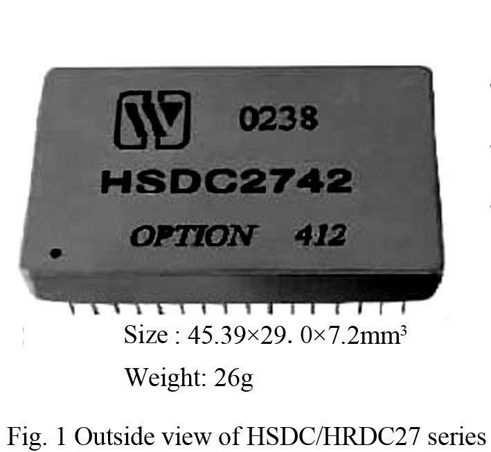
Size: 45.39×29.0×7.2mm2
Weight: 26g
Fig. 1 Outside view of HSDC/HRDC27 series Table 1 Product models
12-bit 14-bit
Synchro Resolver Synchro Resolver
HSDC2742 -412 HRDC2742 -414 HSDC2754 -612 HRDC2754 -414
HRDC2742 -418 HRDC2754 -418
HRDC2742 -618 HRDC2754 -618
HRDC2754 -666
HRDC2754 -614
2. Scope of application
Servo system; antenna system; angle measurement; simulation technology; cannon control; control of industrial machine tools
3. Outline
HSDC/HRDC27 series is the synchro/resolver digital converter for continuous tracking of type II servo loop, it parallely latches and outputs 12-bit or 14-bit natural binary coded data with 32-line dual-in-line metal package, features the advantages of small volume, light weight and high reliability etc., it is widely applied in such automatic control system as radar system, navigation system, etc.
The operating power is +15V and +5V DC power. The input signals are divided into two types: 3-line synchro and excitation signal (SDC converter) or 4-line resolver and excitation signal (RDC converter)The output is binary parallel digital code. Table 2 Rated conditions and recommended operating conditions
Max. absolute rating value Supply voltage Vs: ± 17.25V
Logical voltage VL: +5.5V
Storage temperature range: -55℃~125℃
Recommended operating conditions Supply voltage Vs: ±15V
Supply voltage VL: +5V
Effective value of reference voltage VRef: ±10% of nominal value
Effective value of signal voltage Vi: ±5% of nominal value
Reference frequency f*: 50Hz~2.6kHz
Operating temperature range TA: -40~+85℃,-55~+105℃
Note: * indicates it can be customized as per user’s requirement.
4. Technical performance (Table 2, Table 3)
Table 3 Electric characteristics
Characteristics HSDC/HRDC2742 Enterprise military standard (Q/HW30859-2006) HSDC/HRDC2754 Enterprise military standard (Q/HW30832-2006) Unit Remarks
Converter performance Accuracy ±8.5 ±5.3 Angular minute
Tracking speed 25(min) 12(min) rps At 400Hz excitation
Resolution 12 14 bit
Signal and reference frequency 50~2600 50~2600 Hz Optional*
Signal input voltage 11.8, 26, 90 11.8, 26, 90 V Optional**
Reference input voltage 11.8, 26, 115 11.8, 26, 115 V Optional**
Step response 100 150 ms
Acceleration constant 82000 39000 s-2
Power consumption 0.86max 1.3max W
Busy pulse width 1max 1max µs
Digital output loading capacity 2max 2max TTL
Notes: * For the converter with other operating frequency such as 50Hz, 2kHz etc., its dynamic parameters are different, which can be provided according to user’s need;
** indicates it can be customized as per user’s requirement.
5. Operating principle (Fig. 2)
The synchro input signal (or input signal of resolver) is converted into the orthogonal signal through internal differential isolation:
V1=KE0sinθ sinωt,V2=KE0cosθ sinωt
Where, θ is the simulated input angle.
These two signals and the digital angle φ of internal reversible counter are multiplied in the multiplier of sine and cosine functions and are error treated:
KE0sinθ cosφ sinωt-KE0cosθ sinφ sinωt=KE0sin(θ-φ) sinωt
The signals are sent to voltage controlled oscillator after amplification, phase discrimination, integration filtration, if θ-φ≠0, the voltage controlled oscillator changes the data in the reversible counter with the output pulses until θ-φ becomes zero within the accuracy of the converter, during this process, the converter tracks the change of input angle θ all the time.
Fig.2 Block diagram for operating principle
Transfer function of converter
Closed-loop function
Data transfer method and time sequence
There are two methods for reading the effective data in the converter: synchronous reading and asynchronous reading.
(1) Inhibit mode (synchronous reading):
A: the converter is connected with 16-bit bus. Bysel is connected with logic “1”.
is set to logic “0” from logic “1” (data locking), wait for 1μs; set to logic “0”, the latch inside the converter allows data to be output; read 12-bit or 14-bit data; set Inhibit to logic “1” so as to get ready for reading next valid data (see the time sequence diagram for 16-bit transfer).
B: the converter is connected to 8-bit bus, D1~D8 bit are connected to data bus, and the rest are empty.
is set to logic “0” from logic “1” (data locking), wait for 1μs; set to logic “0”, the latch data inside the converter allows output; if Byse1 is set to logic “1”, the converter directly reads the higher 8-bit data, if Byse1 is set to logic “0”, the converter reads the rest bits, automatically adds zero for incomplete bits; set to logic “1” in order to get ready for reading next valid data (see Fig. 3 and Fig. 4 for 8-bit transfer time sequence).
Fig. 3 Time sequence diagram of 16-bit bus transfer
Fig. 4 Time sequence diagram of 8-bit bus transfer
(2) Busy mode (asynchronous reading)
In asynchronous reading mode, is set to logic “1” or is vacant, whether the internal loop is in the stable state or whether the output data is valid shall be determined through the status of Busy signal Busy. When Busy signal is at high level, it indicates the data is under conversion, and the data at this time is unstable and invalid data; when Busy signal is at low level, it indicates a data conversion has been completed, the data at this time is stable and valid and can be read out. Once high level occurs in Busy during reading, the reading of this time is invalid. In asynchronous reading mode, Busy output is pulse train of TTL level, the width between is related to rotational speed. Likewise, there are also two use methods of 8-bit bus and 16-bit bus, in case of valid data output, data reading is also controlled by , refer to time sequence diagram for data transfer (Fig.5 and Fig.6)
Fig5 Time sequence diagram for 16-bit bus transfer
Fig.6 Time sequence diagram for 8-bit bus transfer
6. MTBF curve (Fig. 7)
Fig. 7 MTBF-temperature curve 7. Pin designation (Fig. 8, Table 3)
Fig. 8 Pins (Bottom view)
(Note: according to GJB/Z299B-98, envisaged good ground condition)
Table 3 Pin designation
Pin Symbol Function Pin Symbol Function
1~14 D1~D14 Digital output 24 Bysel Bit select
15 RLo Excitation signal input 25 NC Leave unconnected
16 RHi Excitation signal input 26 Data gating
17 S4 Signal input 27 Busy Busy pulse output
18 S3 Signal input 28 Data latch control
19 S2 Signal input 29 +15V Power
20 S1 Signal input 30 GND Power ground
21 NC Leave unconnected 31 -15V Power
22 Vel Velocity voltage output 32 +5V Power
23 Case Case ground
Notes: ① For 12-bit converter, leave pin 13 and 14 unconnected.
② For SDC converter, leave pin 17 is unconnected.
③ Power supply: ±15V, +5V, GND, the power shall not be connected reversely, otherwise, devices will be damaged.
④ Binary digital output: it is divided into 12-bit and 14-bit output.
⑤ RHi, RLo: excitation signal input.
⑥ S1, S2, S3, S4: signal input of synchro/resolver (S4 is left unconnected for synchro).
⑦ Busy: Busy signal
This signal indicates whether the binary number output from the converter is valid or not. When Busy is at high level, it indicates the converter is carrying out data conversion, the data output at this time is invalid; when Busy is at low level, the data in the converter has been stable and the data output at this time is valid.
⑧ Data gating
This pin is the input pin of control logic, its function is to output data to the converter to realize three-state control. Low level is valid, the output data of converter occupies the data bus. When it is at high level, the data output pin of converter is in three states, the device does not occupy the bus.
⑨ Data locking control (Inhibit signal )
This pin is the input pin of control logic, its function is to output data externally to the converter to realize optional latching or bypass control.
At high level, the output data of the converter directly outputs without latching; at low level, the output data of the converter is latched, the data is not updated, but the internal loop is not interrupted, and tracking is working all the time. has connected pull-up resistance inside the converter (whether the device uses data bus, i.e. when it outputs the data depends on the state of ).
⑩ Byse1: bit selection end
This is a control end specially designed for connecting the converter with 8-bit data or 16-bit data bus. When the converter is connected with 16-bit data bus, Byse1 is pulled up internally, the converter can directly output 12-bit or 14-bit data; when the converter is connected with 8-bit data bus, Byse1 is at a high level, the converter outputs data of higher 8 bits (D1~D8), when Byse1 is at low level, the converter outputs data of the rest bits (copying the data of the rest bits to bit D1~D8), and automatically fills zero for the data of short bits. It shall be noted that it is only needed to connect D1~D8 when the converter is connected with 8-bit data bus, other data pins are left unconnected.
8. Table of weight values (Table 4)
Table 4 Table of weight values
Bit Angle Bit Angle Bit Angle
1(MSB) 180.0000 6 5.6250 11 0.1758
2 90.0000 7 2.8125 12 (for 12-bit LSB) 0.0879
3 45.0000 8 1.4063 13 0.0439
4 22.5000 9 0.7031 14 (for 14-bit LSB) 0.0220
5 11.2500 10 0.3516
9. Connection diagram for typical application (Fig. 9)
Besides being directly used in precise measurement of rotational angle of the synchro or resolver, the shaft angle converter can also constitute two-speed measurement system or other digital measurement control system of higher precision. Fig. 9 is an example of two-speed system composed of the converter. The two-speed system established on the principle of combination of coarse and precise measurement has a higher conversion precision, Fig.9 shows the two-speed conversion system composed of two synchros (or resolvers) coupled through the gearbox, two SDC converters and a two-speed processor HTSL19, its output reaches 19 bits.
Fig. 9 Application of two-speed system of SDC
10. Package specifications (unit: mm) (Fig. 10)
Fig.10 Package specification
Table 5 Case materials
Case model Header Header plating Cover Cover plating Pin material Pin plating Sealing style Remarks
UP4529- 32a Kovar (4J29) Au Fe-Ni alloy (4J42) Au Kovar (4J29) Au Matched packaging Coating of pin 23 is Au
Note: temperature of the solder pins shall not exceed 300℃ within 10s.
11. Part numbering key (Fig. 11)
Fig.11 Part numbering key
Note: when the above signal voltage and reference voltage (Z) are non-standard, they shall be given as follows:
(e.g. reference voltage 5V and signal voltage 3V shall be expressed as -5/3)
Precautions for use
Supply power correctly, during the power-up, accurately connect the positive and negative poles of power to avoid burnout.
Connection of the converter
±15V, +5V and GND shall be connected to corresponding pins on the converter, notice that the polarities of the power supply must be correct, otherwise, the converter may be damaged. It is recommended to connect 0.1μF and 6.8μF bypass capacitance in parallel between each power supply terminal and ground. Signal and excitation source are allowed to be connected to S1, S2, S3 and S4 and RHi and RLo end within an error of 5%. It is only needed to connect D1~D8 when the converter is connected with 8-bit data bus, other data pins are left vacant.
When the converter is connected to 16-bit data bus, D1~D14 or (D1~D12) shall all be connected.
The signal input shall match the phase of the excitation so that they can be correctly connected with the converter, their phases are as follows:
RHi~RLo: VRsinωt
For the synchro:
For S1~S3: sinθ sinωt
For S3~S2: sin(θ+120o) sinωt
For S2~S1: sin(θ+240o) sinωt
For the resolver:
For S1~S3: sinθ sinωt
For S2~S4: cosθ sinωt
Note: no input signal of RHi, RLo, S1, S2, S3 and S4 is allowed to be connected to other pins for fear of damage of the device.
During the assembly, the bottom of the product shall fit to the circuit board closely so as to avoid damage of pins, and shockproof provision shall be added, if necessary.
When the user places an order for the product, detailed electric performance indexes shall refer to the relevant enterprise standard.
R/D converter (H2S80)
1. Features (see Fig. 1 for outside view, and Table 1 for models)
Optional 10, 12, 14 and 16-bit resolution
Tracking rate: max. 1040 r/sec
Dynamic parameters: designed by user
High input impedance, three-state latch output
40-wire salt fog resistant metal sealed DDIP package
Compatible with ADC2S80 series of American AD company
Size: 53×20×5.3mm2
Weight: 18g
Fig. 1 Outside view of H2S80 2. Scope of application
Missile servo system; flight control electronic system; radar control system; ship navigation system; antenna monitoring; artillery control system; numerical control (CNC) machine tools; robot system.
3. Outline
H2S80 type II servo loop continuous tracking R/D converter is designed and manufactured by adopting MCM process, the kernel device is the special chip developed independently by our company, the pin arrangement is compatible with AD2S80 product of American AD company, 10, 12, 14 and 16-bit (optional resolution) parallel natural binary data latch output, 40-line DIL metal hermetic case package, has the advantages of high accuracy, low power consumption, small volume, light weight and high reliability etc., and can be widely used for electronic control of the system as of airplane, ship, artillery, missile, radar, tank etc. Table 1 Rated conditions and recommended operating conditions
Max. absolute rating value Logical supply voltage VL: 7V
Supply voltage Vs: ± 13.5V
Signal voltage Vi: 2V±20%
Reference voltage: VRef: 2V±20%
Operating frequency f: 50~20000Hz
Storage temperature Tstg: 65~150℃
Recommended operating conditions Logical supply voltage VL: 5±0.5V
Supply voltage Vs: ±12±0.75V
Signal voltage Vi: 2V±10%
Reference voltage: VRef: 2V±10%
Operating frequency f: 50~20000Hz
Operating temperature range (TA): 55~125℃
4. Electrical characteristics (Table 1, Table 2)
Table 2 Electric characteristics
Characteristics H2S80 Unit Characteristics H2S80
Enterprise military standard (Q/HW30974-2007) Unit
Resolution Optional 10, 12, 14 and 16-bit
±21 minuts+1LSB(10 bits) Signal voltage 2V±10% V
±8 minuts+1LSB(12 bits) Reference voltage 2V±10% V
Accuracy ±4 minuts+1LSB(14 bits) bit Digital input level Compatible with TTL
±2 minuts+1LSB(16 bits)
Tracking speed 0~1040 (10 bits) r/sec Digital output level Logic high ≥3.3
Logic low ≤0.7 V
0~260 (12 bits)
0~65 (14 bits)
0~16 (16 bits) Power +12, 12, +5 V
Operating frequency range 50~20000 Hz Power consumption 450 mW
5. Operating principle (Fig. 2 and Fig. 3)
The input signal of synchro (or resolver) is converted into the orthogonal signal through the internal differential isolation:
Vsin-KE0sin(ωt+α) sinθ (sin)
Vcos-KE0sin(ωt+α) cosθ (cos)
Where, θ is the analog input angle.
These two signals and the digital angle φ of internal reversible counter are multiplied in the multiplier of sine and cosine functions and are error treated:
KE0sin(ωt+α) (sinθ cosφ -cosθ sinφ)
i.e. KE0sin(ωt+α) sin(θ-φ)
It is sent to voltage-controlled oscillator after amplification, phase discrimination and integration filtration, if θ-φ≠0, the voltage-controlled oscillator will output the pulses and the reversible counter counts them until θ-φ becomes zero within the accuracy of the converter. In this process, the converter tracks the change of input angle all the time.
Fig.2 Block diagram for operating principle
Reading mode:
Following two methods are available for data transfer:
(1) mode
After 640ns of logic low, the output data is valid, and the converter realizes data transfer through Enable. After Inhibit is released, the system will automatically generate a pulse with its width equal to that of Busy pulse for data updating.
(2) Bust mode:
At the rising edge of Busy pulse, the three-state reversible counter counts; at the descending edge of Busy pulse, it internally generates a latch pulse with its width equal to that of Busy pulse for updating the data of the three-state latch, the time sequence of data transfer is shown in Fig.3, in other words, after 600ns of Busy logic low, the stable transfer of data is valid. In the reading process, once high level occurs in Busy, the reading of this time is invalid. In asynchronous reading mode, Busy output is pulse train of CMOS level, the pulse width is related to rotational speed.
Fig. 3 Time sequence diagram for bus reading
6. MTBF curve (Fig. 4)
Fig. 4 MTBF-temperature curve 7. Pin designation (Fig. 5, Table 3)
Fig. 5 Pins (Bottom view)
(Note: according to GJB/Z299B-98, envisaged good ground condition)
Table 3 Pin designation
Pin Symbol Function Pin Symbol Function Pin Symbol Function
1 Ref/I Reference signal input 15 D7 Digital output 7 29 DG Digital ground ⑧
2 Demo/I Discriminator input 16 D8 Digital output 8 30 SC1 Resolution select input ①
3 Acer/O AC error input 17 D9 Digital output 9 31 SC2
4 cos Cosine signal input 18 D10 Digital output 10 32 NC Leave unconnected
5 AG Analog ground ⑧ 19 D11 Digital output 11 33 Busy Busy signal output ④
6 SG Signal ground ⑧ 20 D12 Digital output 12 34 Direction Counting direction signal output ⑤
7 sin Sine signal input 21 D13 Digital output 13 35 Ripclk Zero-bit signal output ⑥
8 +VS +12V power ⑦ 22 D14 Digital output 14 36 -VS -12V power ⑦
9 D1 Digital output 1 (MSB) 23 D15 Digital output 15 37 Vco/I Voltage-controlled oscillator input
10 D2 Digital output 2 24 D16 Digital output bit 16 (LSB) 38 Inte/I Integrator input
11 D3 Digital output 3 25 +VL +5V power ⑦ 39 Inte/O Integrator output
12 D4 Digital output 4 26 Enable signal input ② 40 Demo/O Discriminator output
13① D5 Digital output 5 27 NC Leave unconnected
14① D6 Digital output 6 28 Static signal input ③
Note: ① SC1 and SC2 for resolution select input, have been connected with pull-up resistance internally.
Resolution SC1 SC2
10 0 0
12 0 1
14 1 0
16 1 1
② enable signal input, this pin is the logic input pin of data gating control, its function is to carry out three-state control externally on the output data of the converter. Low level is valid, the output data of converter occupies the data bus. When it is at high level, the data output pin of converter appears in high impedance state, the device does not occupy the bus. Enable and release delay time is 600ns(max).
③ static signal input, this pin is the input pin of data latch control logic, its function is to carry out latch or bypass select control of the output data of the converter. At high level, the output data of the converter is directly output without latching; at low level, the output data of the converter is latched, the data is not updated, but the internal loop is not interrupted, and tracking is working all the time, has been connected with pull-up resistance internally. After 600ns (max) delay of descending edge of the static signal, the data becomes stable (whether the device occupies the data bus or not, i.e. when does it output the data depends on the state of Enable).
④ “Busy” signal output, this signal indicates whether the binary code output of the converter is valid or not. When Busy is at high level, it indicates the converter is carrying out data conversion, the data output at this time is invalid; when Busy is at low level, it indicates that the data in the converter has been stable and the data output at this time is valid, the pulse width is 400ns.
⑤ Direction: counting direction signal output, high level indicates the converter is adding the count, and low level indicates the converter is deducting the count.
⑥ RIPCLK: Zero signal output: when the output data increases from all “1” to all “0”, or the output data decreases from all “0” to all “1”, the output is positive pulse, the pulse width is 200μs.
⑦ Power: +VS
+12V power
12mA
-VS -12V power 18mA
+VL +5V power 10mA
⑧ Ground: Analog ground AG and digital ground DG needs to be externally connected to power ground.
8. Connection diagram for typical application (Fig. 6)
Fig. 6 Connection diagram for typical application
(1) Setting of filter
15kΩ≤R1=R2≤56kΩ
C1=C2= (R1 unit: Ω; fRef is the frequency of excitation source signal, unit: Hz)
(2) Setting of gain
R4=
EDC=160×10-3
=40×10-3
=10×10-3
=2.5×10⁻³ (10-bit resolution)
(12-bit resolution)
(14-bit resolution)
(16-bit resolution)
(3) Reference signal input
R3=100kΩ
C3>
(4) Setting of max. tracking rate
T is the max. tracking rate (unit: r/sec), but should not exceed 1/16 of the reference frequency. In order to make the product be at max. tracking rate, and angular velocity voltage reach 8V, it is required:
R6=
p=1024
=4096
=16384
=65536 (10-bit resolution)
(12-bit resolution)
(14-bit resolution)
(16-bit resolution) Table 4 Setting of tracking rate
Resolution Proportion of reference frequency to bandwidth frequency fBW
10 2.5:1
12 4:1
14 6:1
16 7.5:1
(5) Setting of bandwidth select loop
The selected proportion of reference frequency to bandwidth frequency of the product should not be less than the specified in Table 4.
For example: select 50Hz for 14-bit resolution and 400Hz reference frequency of the product.
C4= (unit of R6: kΩ)
C5=5×C4
R5=
(6) Setting of VCo filter
C6=470pF,R7=68Ω
(7) Zero setting
In order to eliminate zero drift of the product, it can be adjusted using the potentiometer R9, the method is: short circuit pin 4 and 1 of the product, short circuit pin 7 and 6 (equivalent to 0o input angle), regulate potentiometer R9 to make the output data of the product all to zero.
For the power supply connected to +VS and -VS pin, its voltage should be ±12V, and should not be reversely connected. The digital logic power VL is connected to the location of +5V. Between the power and ground, 0.1µF ceramic capacitor and 6.8µF electrolytic capacitor should be connected in parallel.
9. Package specifications (unit: mm) (Fig. 7, Table 5 and 6)
Fig. 7 Outside view and dimensions of package Table 5 Package specification
Symbol Value
Min. Nominal Max.
A 5.5
Φb 0.35 0.55
D 53.8
E 20.0
e 2.54
e1 15.24
L 5
Table 6 Case materials
Case model Header Header plating Cover Cover plating Pin material Pin plating Sealing style Remarks
UP5320- 40 4J42 Ni coating 4J42 Chemical Ni coating 4J42 Au coating Matched packaging Base plus three solid glass beads
Note: temperature of the solder pins shall not exceed 300℃ within 10s.
10. Part numbering key (Fig. 8)
Fig. 8 Part numbering key
Precautions for use
Supply power correctly, during the power-up, accurately connect the positive and negative poles of power to avoid burnout.
During the assembly, the bottom of the product shall fit to the circuit board closely so as to avoid damage of pins, and shockproof provision shall be added, if necessary.
Do not bend the pinouts to prevent the insulator from breaking, which affect the sealing property.
When the user places an order for the product, detailed electric performance indexes shall refer to the relevant enterprise standard.
Synchro/Resolver to Digital Converter
(HSDC/HRDC1459 Series)
1. Features (see Fig. 1 for outside view, and Table 1 for models)
Internal differential isolation conversion
16-bit resolution
Accuracy: 2 angular minutes
Three-state latch output
High continuous tracking speed
36-wire salt fog resistant metal sealed DDIP package
Pin-To-Pin compatible with Model SDC14560 of DDC company
Size: 48.2×20×5.3mm3; weight: 17g
Fig.1 Outside view of HSDC/HRDC1459 Series
2. Scope of application
Military servo control system; antenna monitoring; radar control system; navigation system for naval vessels; cannon control system; flight instrument system; aviation electronic system; computerized numeric control (CNC) machine; robot technology.
3. Outline
HSDC/HRDC1459 series synchro/resolver to digital converter is a hybrid integrated conversion device for continuous tracking designed on the principle of model II servo. This series products are designed and manufactured by MCM process, the core elements adopt special chip developed independently by our institute. The pin arrangement is compatible with SDC14560 series products of American DDC company, 16-bit parallel natural binary code data latch output, 36-wire DIP totally sealed metal package, have the advantages of high precision, small volume, low power consumption, light weight and high reliability etc., and can be widely used in important strategic and tactic weapons such as aircraft, naval vessel, cannon, missile, radar, tank, etc.
4. Electrical performance (Table 1, Table 2)
Max. absolute rating value Logical supply voltage VL: +7V
Supply voltage Vs: ± 17.5V
Signal voltage Vi: rated value ±20%
Reference voltage VRef: rated value ±20%
Operating frequency f: rated value ±20%
Storage temperature Tstg: -65~150℃
Recommended operating conditions Logical supply voltage VL: 5±0.5V
Supply voltage Vs: ¡À15¡À0.75V
Signal voltage Vi: rated value ±10%
Reference voltage VRef: rated value ±10%
Operating frequency f*: rated value ±10%
Operating temperature range (TA): -55~125℃
Note: * indicates it can be customized as per user’s requirement.
Table 2 Electric characteristics
Characteristics Condition
(VS=±15V, VL=+5V) HSDC14569 Series
Military standard (Q/HW20725-2006)
Min. Max.
Resolution Binary parallel digital code 16-bit
Accuracy ±10% of signal voltage, reference voltage and fluctuation range of operating frequency -2 angular minutes +2 angular minutes
Range of reference frequency 50Hz 2600Hz
Range of reference voltage 2V 115V
Reference input impedance 4.4kΩ 129.2kΩ
Range of signal voltage 2V 90V
Signal input impedance 4.4kΩ 102.2kΩ
Signal/reference phase shift -70o +70o
Input logic level Logic “1” ≥3.3V Logic “0” ≤0.8V
input 0 0.8V
input 0 0.8V
input 0 0.8V
Output logic level Logic “1” ≥3.3V Logic “0” ≤0.8V
Digital angle code output Logic “1” ≥3.3V Logic “0” ≤0.8V
Converting busy signal (CB) output 200ns 600ns
Fault detection Bit output Logic “0” indicates fault
Loading capacity 3TTL
Tracking speed 2.5 r/sec
Acceleration constant 12500
Settling time 850ms
Angular velocity voltage (Vel) output -10V +10V
Current Vs=+15V 10mA
Vs=-15V 15mA
VL=+5V 20mA
5. Step response
When a step in the input signal or initial power-on happens, the response will be inhibited due to the limitation of maximum tracking rate. The oscillation process of the output digital angle is shown in Fig. 2:
Fig.2 Curve of step response
6. Operating principle (Fig. 3)
The input signal of synchro (or resolver) is converted into the orthogonal signal through the internal differential isolation:
Vsin=KE0sin(ωt+α) sinθ (sin)
Vcos=KE0sin(ωt+α) cosθ (cos)
Where, θ is the analog input angle.
These two signals and the digital angle φ of internal reversible counter are multiplied in the multiplier of sine and cosine functions and are error treated:
KE0sin(ωt+α) (sinθ cosφ -cosθ sinφ)即KE0sin(ωt+α) sin(θ-φ)
This signal is sent to voltage-controlled oscillator after amplification, phase discrimination, integration filtration. If θ-φ≠0, voltage controlled oscillator will output pulses and the reversible counter counts them until θ-φ=0 within the accuracy of the converter. In this process, the converter tracks the change of input angle all the time.
Reading mode:
Following two methods are available for data transfer:
(1) mode
After 640ns of logic low, the output data is valid, and the converter realizes data transfer through and . After Inhibit is released, the system will automatically generate a pulse with its width equal to that of Busy pulse for data updating.
(2) Bust mode:
At the rising edge of Busy pulse, the three-state reversible counter counts; at the descending edge of Busy pulse, it internally generates a latch pulse with its width equal to that of Busy pulse for updating the data of the three-state latch, the time sequence of data transfer is shown in Fig. 4, in other words, after 600ns of Busy logic low, the stable transfer of data is valid. In asynchronous reading mode, Busy output is a pulse train of CMOS level, the widths of its high and low level depend on operating frequency and rotating speed of the device selected.
Fig. 3 Operating principle block diagram
Fig.4 Time sequence of data transfer
7. MTBF curve (Fig. 5)
Fig. 5 MTBF-temperature curve 8. Pin designation (Fig. 6, Table 3)
Fig. 6 Pins (Bottom view)
(Note: according to GJB/Z299B-98, envisaged good ground condition)
Table 3 Pin designation
Pin Symbol Meaning Pin Symbol Meaning
1 S1 Resolver input S1 (or synchro input S1) 25 Enable control of low 8-bit digits
2 S2 Resolver input S2 (or synchro input S2) 26 Enable control of high 8-bit digits
3 S3 Resolver input S3 (or synchro input S3) 27 RIPCLK Zero-bit signal output
4 S4 Resolver input S4 (leave unconnected) 28 VL +5V power
5~18 D1~D14 Digital output 1 (MSB)-14 29 GND Ground
19 RHi High end of reference signal input 30 NC Vacant
20 RLo Low end of reference signal input 31 -Vs -15V power
21 D15 Digital output 15 32 -15V +15V power
22 D16 Digital output 16 (LSB) 33 Static signal input
23 Vel Angular velocity voltage signal output 34 Fault detection bit output
24 GB Busy signal output 36-36 NC Vacant
Notes: D1~D16 Parallel binary system digital angle code output end
S1, S2, S3, S4 Signal input of resolver (or synchro)
RHi High end of reference signal input
RLo Low end of reference signal input
Lower 8-bit digit enabled signal input, this pin is the logic input pin of data gating control, its function is to carry out three-state control externally on the lower 8-bit output data of the converter. Low level is valid, the low 8-bit output data of converter occupies the data bus. When it is at high level, the low 8-bit data output pin of converter appears in high impedance state, the device does not occupy the bus. Enable and release delay time is 600ns(max).
high 8-bit digit enabled signal input, this pin is the logic input pin of data gating control, its function is to carry out three-state control externally on the higher 8-bit output data of the converter. Low level is valid, the high 8-bit output data of converter occupies the data bus. When it is at high level, the high 8-bit data output pin of converter appears in high impedance state, the device does not occupy the bus. Enable and release delay time is 600ns(max).
static signal input, this pin is the input pin of data latch control logic, its function is to carry out latch or bypass select control of the output data of the converter. At high level, the output data of the converter is directly output without latching; at low level, the output data of the converter is latched, the data is not updated, but the internal loop is not interrupted, and tracking is working all the time, has been connected with pull-up resistance internally. After 600ns (max) delay of descending edge of static signal, the data becomes stable (whether the device occupies the data bus, i.e. when does it output the data depends on the state of and ).
CB “Busy” signal output, this signal indicates whether the binary code output of the converter is valid or not. After the change in angular input reaches 0.33 angular minute, CB end outputs a positive pulse with a width of 400ns (typical), when CB is at high level, it means the converter is under conversion, at this time, the output data is invalid; after the falling edge of CB signal delays for 600ns (max.), the data becomes stable, at this time, the output updated data is valid.
fault detection bit output, high level indicates normal working of the converter, in the event that the signal wire is broken or the converter fails to track normally, this bit changes into low level from high level.
RIPCLK: Zero signal output R.C: when the output data increases from all “1” to all “0”, or the output data decreases from all “0” to all “1”, the output is positive pulse, the pulse width is 200μs.
VL, VS, VS Incoming end of power supply
GND Ground wire incoming end
Hints:
① Pin voltage shall not exceed 20% of rated value.
② The voltage of power supply shall not exceed the specified range.
③ Do not connect reference RHi and RLo to other pins.
④ For the power supply connected to +VS and -VS pin, its voltage shall be ±15V, and shall not be reversely connected. The digital logic power supply VL is connected to +5V. Between the power and ground, 0.1µF ceramic capacitor and 6.8µF electrolytic capacitor should be connected in parallel.
⑤ Reference signals are connected to RHi and RLo. In the case of synchro, signals are connected to S1, S2, and S3 as per the following conventions:
sin(ωt+α) sinθ
sin(ωt+α) sin(θ+120o)
sin(ωt+α) sin(θ+240o)
⑥ In the case of resolver, signals are connected to S1, S2, S3 and S4 as per the following conventions:
sin(ωt+α)sinθ
sin(ωt+α) cosθ
Pins of CB, , and shall all be connected as described for the above data transfer.
9. Table of weight values (Table 4)
Table 4 Table of weight values
Bit Angle/bit Angular minute/bit Bit Angle Angular minute/bit Bit Angle Angular minute/bit
1(MSB) 180.0000 10800 7 2.8125 168.75 13 0.0439 2.64
2 90.0000 5400 8 1.4063 84.38 14 0.0220 1.32
3 45.0000 2700 9 0.7031 42.19 15 0.0110 0.66
4 22.5000 1350 10 0.3516 21.09 16(LSB) 0.0055 0.33
5 11.2500 675 11 0.1758 10.55
6 5.6250 387.5 12 0.0879 5.27
10. Connection diagram for typical application (Fig. 7) 11. Package specifications (unit: mm) (Fig. 8, Table 5)
Fig. 7 Connection diagram for typical application
Fig. 8 Outside view and dimensions of package
Table 5 Case materials
Case model Header Header plating Cover Cover plating Pin material Pin plating Sealing style Remarks
UP4820- 36A 4J42 Ni coating 4J42 Chemical Ni coating 4J42 Au coating Matched packaging Base plus three solid glass beads
12. Part numbering key (Fig. 9)
Fig. 9 Part numbering key
Note: when the above signal voltage and reference voltage (Z) are non-standard, they shall be given as follows:
(e.g. reference voltage 5V and signal voltage 3V are expressed as 5/3)
Precautions for use
Supply power correctly, during the power-up, accurately connect the positive and negative poles of power to avoid burnout.
During the assembly, the bottom of the product shall fit to the circuit board closely so as to avoid damage of pins, and shockproof provision shall be added, if necessary.
Do not bend the pinouts to prevent the insulator from breaking, which affect the sealing property.
When the user places an order for the product, detailed electric performance indexes shall refer to the relevant enterprise standard.
Synchro/Resolver to Digital Converter
(MSDC/MRDC37 series)
1. Features (see Fig. 1 for outside view, and Table 1 for models)
High accuracy
Small volume
High tracking speed
Uninterrupted tracking during data transfer
Three-state latch output
Low power consumption
Size: 50.8×50.8×10mm2
Weight: 48g
Fig.1 Outside view of MSDC/MDRC37 series 2. Scope of application
Servo mechanism; antenna monitoring; navigation system; artillery control; industrial control; robot system; radar control system.
3. Outline
MSDC/MRDC37 series are 16-bit digital converter to synchro/resolver. The input signal is divided into four-wire resolver and excitation signal or three-wire synchro and excitation signal. The output signal is parallel natural binary code buffered through three-state latch and compatible with TTL level.
The product applies second-order servo circuit with small volume and light weight, and the user can use it very conveniently by controlling signal pins.
4. Technical performance (Table 1, Table 2)
Table 1 Rated conditions and recommended operating conditions
Max. absolute rating value Supply voltage +VS: 12.5~17.5V
Supply voltage Vs: 17.25~12.5V
Logical supply voltage VL: 7V
Storage temperature range: -40~+100℃
Recommended operating conditions Supply voltage +VS: 15V±5%
Supply voltage Vs: 15V±5%
Logical voltage VL: 5V±5%
Reference voltage (effective value) VRef: nominal value ±10%
Signal voltage (effective value) Vi: ±10% of nominal value
Reference frequency f*: nominal value ±10%
Operating temperature range TA: 40℃~85℃
Note: * indicates it can be customized as per user’s requirement.
Table 2 Electric characteristics
Characteristics Condition
(40~+85℃)
(Unless otherwise specified) (MSDC/MDRC37 series)
Unit
Min. Max.
Resolution/RES 0~360º 12 16 bit
Tracking rate/St① 3 36 r/sec
High output level/VOH TA=25℃ 2.4 V
Low output level/VOL TA=25℃ 0.8 V
Power consumption/ PD TA=25℃ 1.3 W
Vel linearity/ERI TA=25℃ 1.0 %
Range of reference voltage 2 115 V
Range of signal voltage 2 90 V
Frequency range 30 2600 Hz
Accuracy ±3 ±8.5 Angular minute
Note: ① the tracking speed is 3 rps for 16-bit resolution and 36 rps for 12-bit resolution; St can be designed according to the user’s requirement.
5. Operating principle (Fig. 2)
The synchro input signal (or input signal of resolver) is converted into the orthogonal signal through internal differential isolation:
V1=KE0sinθ sinωt,V2=KE0cosθ sinωt
Fig.2 Block diagram for operating principle
Where, θ is the analog input angle.
These two signals and the digital angle φ of internal reversible counter are multiplied in the multiplier of sine and cosine functions and are error treated:
K·E0sinθ cosφ sinωt-KE0cosθ sinφ sinωt=KE0sin(θ-φ) sinωt
The signals are sent to voltage controlled oscillator after amplification, phase discrimination, integration and filtration, if θ-φ≠0, the voltage controlled oscillator changes the data in the reversible counter with the output pulses until θ-φ becomes zero within the accuracy of the converter, during this process, the converter tracks the change of input angle θ all the time.
Transfer function of the converter is shown in Fig. 3.
Fig. 3 Function transfer of the converter
闭环函数
Data transfer method and time sequence
There are two methods for reading the effective data in the converter: synchronous reading and asynchronous reading.
(1) Inhibit mode (synchronous reading):
A: the converter is connected with 16-bit bus. B


 X
X


 Gold Supplier