|
Absolute maximum rating |
Operating conditions |
|
Input Voltage: 475V Output Power: 440W,165W,330W Storage temperature: -65~135℃ Lead welding temperature(10s): 300℃ Junction Temperature:<150℃ |
Input voltage:155~425V Working temperature(Tc):-55~100℃ |
|
No. |
Character |
Symbol |
Conditions ( Unless otherwisespecified ,-55℃≤Tc≤125℃,VIN=270V±10V) |
Limit value |
Unit |
||||
|
min |
max |
||||||||
|
1 |
Input under-voltage/V |
turn-on voltage |
VINL-ONT
VINL-OFF |
TA=25℃ |
146 |
154 |
V |
||
|
Turn-off voltage |
TA=25℃ |
135 |
145 |
V |
|||||
|
2 |
Output Voltage |
Vo |
Full-load |
TA=25℃ |
4.95 |
5.05 |
V |
||
|
Tc=-55℃ TC=100℃ |
4.925 |
5.075 |
|||||||
|
3 |
Output Current |
Io |
Vin=155V~425V |
- |
80 |
A |
|||
|
4 |
Voltage regulation |
Sv |
155V 425V,Full-load TA=25℃、 Tc=-55℃和 TC=100℃ |
- |
±0.30 |
% |
|||
|
5 |
Load regulation |
S1 |
No-load Full-load TA=25℃、 Tc=-55℃和 TC=100℃ |
- |
±0.30 |
% |
|||
|
6 |
Output voltage regulation range a |
VTR |
TA=25℃,50% load |
-20 |
10 |
% |
|||
|
7 |
Output ripple voltage |
VPP |
BW≤20MHz, full-load, peak-peak TA=25℃、 Tc=-55℃ TC=100℃ |
- |
400 |
mV |
|||
|
8 |
Output over-voltage protection point |
VOVP |
TA=25℃,design guarantee |
5.6 |
6.9 |
V |
|||
|
9 |
Output current for over-current protection |
Iimax |
TA=25℃ |
88 |
112 |
A |
|||
|
10 |
Capacitive Load |
Co |
TA=25℃,Full-load |
- |
10000 |
μF |
|||
|
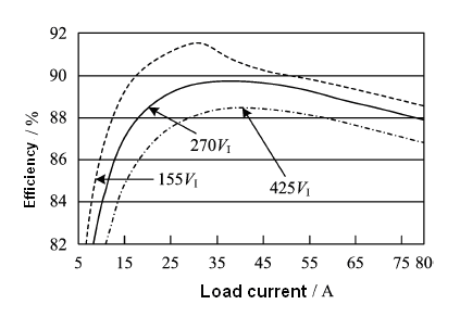
11 |
efficiency |
η |
Vin=270V, Full-load, TA=25℃ |
88 |
- |
% |
|||
|
a test only be needed when identified inspection or parameters are effected by changing process; b design guarantee, do not require test |
|||||||||
|
characteristics |
Conditions ( Unless otherwisespecified ,-55℃≤Tc≤125℃,VIN=270V±10V) |
criteria |
|
Using function |
ON/OFF voltage is over 2.4V, TA=25℃, |
No output |
|
ON/OFF voltage is lower than 0.7V or hung in the air, TA=25℃ |
Normal Output |
|
No. |
characteristics |
Symbol |
conditions ( Unless otherwisespecified ,-55℃≤Tc≤125℃,VIN=270V±10V) |
Limit value |
Unit |
||||
|
min |
max |
||||||||
|
1 |
Input under-voltage/V |
turn-on voltage |
VINL-ONT
VINL-OFF |
TA=25℃ |
145 |
155 |
V |
||
|
Turn-off voltage |
TA=25℃ |
133 |
147 |
V |
|||||
|
2 |
Output voltage |
Vo |
Full-Load |
TA=25℃ |
14.85 |
15.15 |
V |
||
|
Tc=-55℃ TC=100℃ |
14.775 |
15.225 |
|||||||
|
3 |
Output current |
Io |
Vin=155V~425V |
- |
10 |
A |
|||
|
4 |
Voltage regulation |
Sv |
155V 425V,Full-load TA=25℃、 Tc=-55℃和 TC=100℃ |
- |
±0.30 |
% |
|||
|
5 |
Load regulation |
S1 |
No-load Full-load TA=25℃、 Tc=-55℃和 TC=100℃ |
- |
±0.30 |
% |
|||
|
6 |
Output voltage regulation range a |
VTR |
TA=25℃,50% load
|
-20 |
10 |
% |
|||
|
7 |
Output ripple voltage |
VPP |
BW≤20MHz, full-load, peak-peak TA=25℃、 Tc=-55℃和 TC=100℃ |
- |
120 |
mV |
|||
|
8 |
Output over-voltage b protection point |
VOVP |
TA=25℃,design guarantee |
115 |
137 |
V |
|||
|
9 |
Output current for over-current protection |
Iimax |
TA=25℃ |
11 |
14 |
A |
|||
|
10 |
Capacitive Load |
Co |
TA=25℃,Full-load |
- |
2000 |
μF |
|||
|
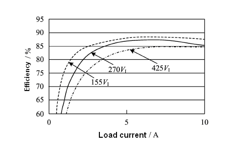
11 |
efficiency |
η |
Vin=270V, Full-load , TA=25℃ |
85 |
- |
% |
|||
|
a test only be needed when identified inspection or parameters are effected by changing proces;b design guarantee, do not require test |
|||||||||
|
characteristics |
Conditions ( Unless otherwisespecified ,-55℃≤Tc≤125℃,VIN=270V±10V) |
criteria |
|
Using function |
ON/OFF voltage is over 2.4V, TA=25℃ |
No output |
|
ON/OFF voltage is lower than 0.7V or hung in the air, TA=25℃ |
Output voltage is Normal |
|
No. |
Character |
Symbol |
( Unless otherwisespecified ,-55℃≤Tc≤125℃,VIN=270V±10V) |
Limit value |
Unit |
||||
|
min |
max |
||||||||
|
1 |
Input under-voltage/V |
turn-on voltage |
VINL-ONT
VINL-OFF |
TA=25℃ |
145 |
155 |
V |
||
|
Turn-off voltage |
TA=25℃ |
133 |
147 |
V |
|||||
|
2 |
Output Voltage |
Vo |
Full-load |
TA=25℃ |
47.52 |
48.48 |
V |
||
|
Tc=-55℃ TC=100℃ |
47.280 |
48.720 |
|||||||
|
3 |
Output Current |
Io |
Vin=155V~425V |
- |
6.3 |
A |
|||
|
4 |
Voltage regulation |
Sv |
155V 425V,Full-load TA=25℃、 Tc=-55℃TC=100℃ |
- |
±0.30 |
% |
|||
|
5 |
Load regulation |
S1 |
No-load Full-load TA=25℃、 Tc=-55℃TC=100℃ |
- |
±0.30 |
% |
|||
|
6 |
Output Voltage trimming range |
VTR |
TA=25℃,50% Load |
-20 |
10 |
% |
|||
|
7 |
Output ripple voltage |
VPP |
BW≤20MHz, full-load, peak-peak TA=25℃、 Tc=-55℃ TC=100℃ |
- |
700 |
mV |
|||
|
8 |
Output over-voltage protection point |
VOVP |
TA=25℃,design guarantee |
55.8 |
64.2 |
V |
|||
|
9 |
Output current for over-current protection |
Iimax |
TA=25℃ |
6.9 |
9.2 |
A |
|||
|
10 |
Capacitive Load |
Co |
TA=25℃,Full-load |
- |
1000 |
μF |
|||
|
11 |
Efficiency |
η |
Vin=270V,Full-load, TA=25℃ |
89 |
- |
% |
|||
|
a test only be needed when identified inspection or parameters are effected by changing processb design guarantee, do not require test |
|||||||||
|
characteristics |
conditions ( Unless otherwisespecified ,-55℃≤Tc≤125℃,VIN=270V±10V) |
criteria |
|
Using function |
ON/OFF voltage is over 2.4V, TA=25℃ |
No output |
|
ON/OFF voltage is lower than 0.7V or hung in the air, TA=25℃ |
Output voltage is Normal |
|
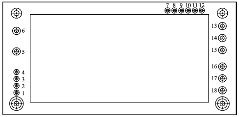
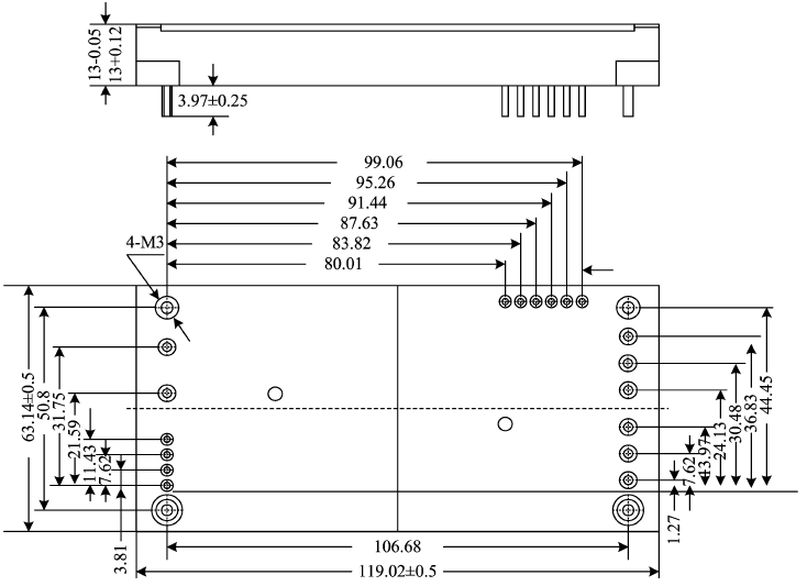
Pin |
Symbol |
Designation |
|
1 |
SyncIn |
Synchronizing signal Input |
|
2 |
SyncOut |
Synchronizing signal Output |
|
3 |
ON/OFF(+) |
Positive Enabling(relative to ON/OFF(-)) |
|
4 |
ON/OFF(-) |
Negative Enabling(isolation common) |
|
5 |
Vin(+) |
Positive Input |
|
6 |
Vin(-) |
Negative Input |
|
7 |
Vaux |
Auxiliary power output(relative to output common) |
|
8 |
Start Sync |
Synchronizing signal start
|
|
9 |
I Share |
Paralleled current sharing Signal |
|
10 |
TRIM |
Output voltage regulation
|
|
11 |
SENSE(+) |
Positive Output Induction |
|
12 |
SENSE(-) |
Negative Output Induction |
|
13 |
Vout(-) |
Negative Output |
|
14 |
Vout(-) |
Negative Output |
|
15 |
Vout(-) |
Negative Output |
|
16 |
Vout(+) |
Positive Output |
|
17 |
Vout(+) |
Positive Output |
|
18 |
Vout(+) |
Positive Output |
|
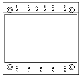
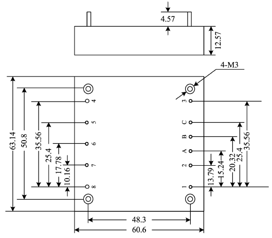
Pin |
Symbol |
Designation |
|
1 |
Vin+ |
Positive Input |
|
2 |
ON/OFF |
Positive Enabling |
|
A |
ClockSync |
Synchronizing signal |
|
B |
StartSync |
Synchronizing start |
|
C |
Ishare |
Paralleled current sharing Signal |
|
3 |
Vin- |
Negative Input |
|
4 |
Vo- |
Negative Output |
|
5 |
S- |
Negative Output Induction |
|
6 |
Trim |
Output voltage regulation |
|
7 |
S+ |
Positive Output Induction |
|
8 |
Vo+ |
Positive Output |

Subscribe to our weekly newsletter and receive exclusive offers on products you love!
 X
X


 Gold Supplier