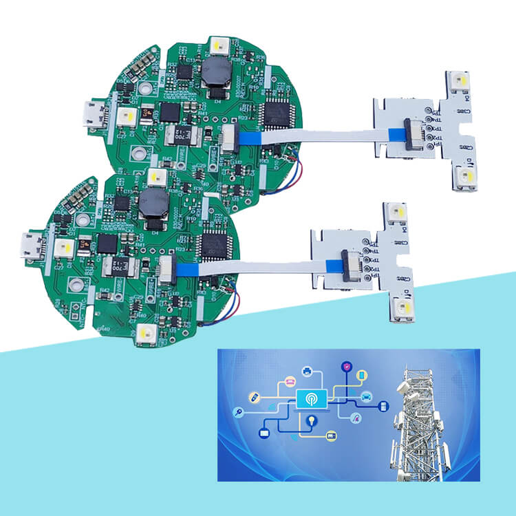
PCBA for fiber optic transceivers and switch electronics. Demands are typically signal integrity and thermal management.
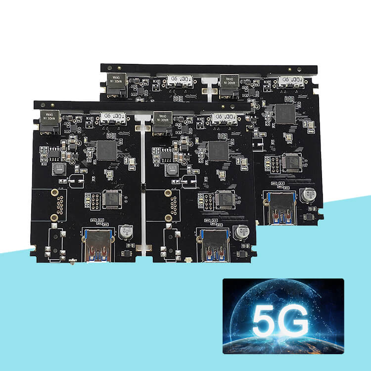
A very clear direction of 5G PCB is high-frequency and high-speed materials and boards. Traditional FR4 materials can no longer meet the needs of high-frequency transmission. In terms of material selection, the Dk (dielectric constant) and Df (dissipation factor) of PCB products must be small.
Generally, boards with a Dk value of less than 3.5 and a Df of less than 0.01 are selected. At the same time, multi-level HDI products and even products that are interconnected in any order will be promoted. For example, the Apple mobile phone PCB adopts 10-layer arbitrary-level hole interconnection, and the overall stacking scheme of multi-board interconnection in the Z direction.
The advantages of space saving and high integration are obvious in the PCB product of this sandwich stacking scheme.


Product advantages:
1. High frequency
2. high speed,
3. space saving,
4. high integration,
5. small motherboard area,
6. high precision and strong durability
7. uniform temperature
8. efficient heat transfer


 X
X