HSA51 Pulse Width Modulation Amplifiers

Sales HSA51 Pulse Width Modulation Amplifiers

HSA51 is a type of pulse width modulation amplifier(PWM Amplifier). It can provide 5A continuous output current to the load;the whole bridge structure can work in a wide voltage range,all the high-end and low-end switching drive control circuit,PWM pulse width modulation circuit are integrated with the product. 
  • Max.Input Vol : 28V
  • Max Current : 5A
  • Function : BRUSHED DC MOTOR CONTROLLER

Product Detail  

1. Features

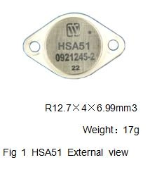
Compatible with APEX SA51、MSK MSK4201

Continuous output current 5A

Peak current  7A

TTL Width square wave signal input

Input inhibit function
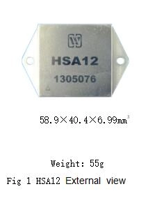
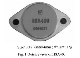
TO-3 Package


2. Scope of application of HSA51 Pulse Width Modulation Amplifier

DC motor drive control
Drive reactive load

3. Descriptions of HSA51 Pulse Width Modulation Amplifier

HSA51 is a type of pulse width modulation amplifier. It can provide 5A continuous output current to the load;the whole bridge structure can work in a wide voltage range,all the high-end and low-end switching drive control circuit,PWM pulse width modulation circuit are integrated with the product. Complete input circuit drive and power amplification wide adjustable square wave signal by  external PID loop speed and position control systems can be completed. Input signal to realize ban  on  internal H bridge switching off.
The series of the products are made of thick film hybrid integrated process, metal sealed shell package. Product design and manufacturing to meet the MIL-STD and detailed specifications of the product requirements, the highest quality level of H-class.

4. Technical Specifications of HSA51 Pulse Width Modulation Amplifier

Table 1 Rated conditions and Recommended operating conditions

Absolute maximum rating

Recommended operating conditions

Supply voltage+VS:80V

Supply voltage+VCC:16V

internal power loss:120W

Storage temperature:-65~+150℃

Enable input voltage(DIS):0~VCC


Supply voltage+VS:28V

Supply voltage+VCC:12V

Input voltage,+V1:0V~5V

Enable input voltage(DIS):0~5V

operating temperature:-55~+125℃


Table 2 electrical characteristics

No

Character

Conditions

VS=28V±1.4V

VCC=12V±1V

RL=1KΩ

RSENSE A、RSENSE BGND

-55℃≤Tc≤125℃

HSA51

Symbol

min

Typical value

max

1

Static current

No signal, VCC=12V±1V

Inhibite terminating

-

18

mA

2

Turn-on voltage

IO=5A

-

2.4

V

3

Shut-off leakage current

output shutoff,Vs=70V no load

-

250

μA

4

Operating current

TC=25℃

FPWM=45KHZ TTL level

-

60

mA

5

Input threshold level

Increased input to A or B status changes

0.8

2.7

V

6

Inhibite  function

TC=25℃

INH add VINTH≥3.6V(inhibite voltage)

FPWM=45KHZ

A or B output shutoff

V


5. Lead function descriptions of HSA51 Pulse Width Modulation Amplifier

Lead function descriptions
Fig  2 upward view

Table 3  Pin Designations

No

symbol

Designation

No

symbol

Designation

1

+VS

Power Supply

5

GND

Ground

2

BOUT

Output B

6

Input

TTL square wave input

3

+VCC

+12V Power

7

AOUT

Output A

4

Disable

Forbidden voltage

8

RSENSE

Inductor


6. Circuit block diagram of HSA51 Pulse Width Modulation Amplifier


Circuit block diagram
Fig  3  Circuit block diagram

7. Typical Connection Diagram of HSA51 Pulse Width Modulation Amplifier

R1、R2 are sampling resistors,According to the current requirements can be   determined by the system.

Typical Connection Diagram
Fig 4 Typical connection diagram

7.1 Power supply bypass
HSA51 power supply should have plenty of bypass to ensure its correct operation, or it may be unstable, reduces efficiency and output maybe oscillations. The VS power supply should add a 1μF ceramic capacitor and parallel a low ESR value of bypass capacitor , the size of at least selected 10μf/ A .The VCC is the same need to parallel a 0.1 μF ceramic capacitor and a low ESR value of 6.8μF-10μF bypass capacitor . All bypass capacitors should be connected as close as possible to the corresponding power source.

8 Package Specifications of HSA51 Pulse Width Modulation Amplifier

Package outline is shown as in fig 5.
Package Specifications
Fig5 package outline drawing

Form 4  Package Outline

Symbol

Data/mm


Min

Typical

Min

A

-

-

6.35

A1

-

-

2.70

Φb

0.90

-

1.10

ΦD

-

-

25.65

ΦD1

-

-

22.20

α

-

40°

-

X1

29.95

-

30.35

X

-

-

39.22

L

11.70

-

-

ΦP

3.80

-

4.20


Note :Consistency in identification and quality Detection, should detect all sizes .
In the group A lot-by-lot testing,only test ΦD、ΦD1、X、X1、A、L.

Application Notes please refer to the appendix, must read it carefully
Leave A Message
If you are interested in our products and want to know more details,please leave a message here,we will reply you as soon as we can.
X

Home

Supplier

Leave a message

Leave a message

If you are interested in our products and want to know more details,please leave a message here,we will reply you as soon as we can.